
Market Report · July 20, 2026

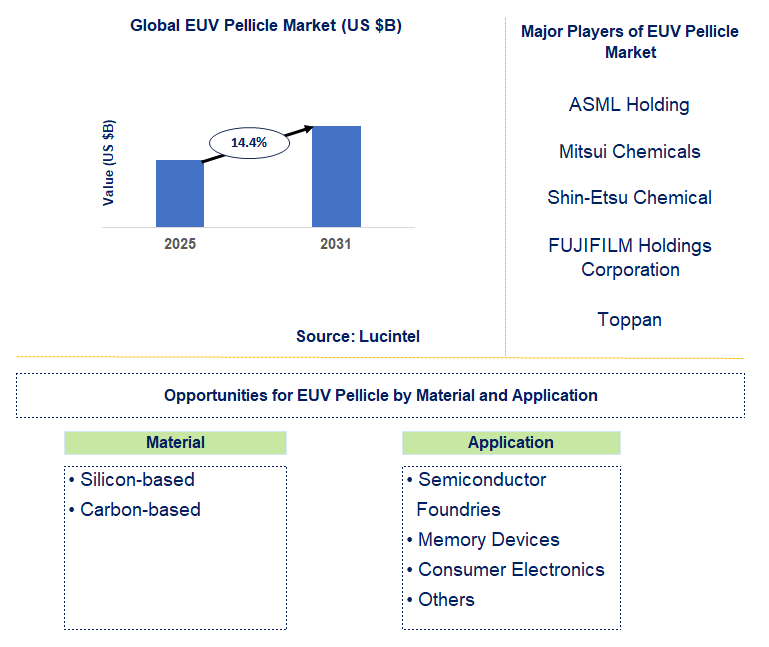
Key data points: The growth forecast = 14.4% annually for the next 7 years. Scroll below to get more insights. This market report covers trends, opportunities and forecasts in EUV pellicle market to 2031 by material (silicon-based and carbon-based), application (semiconductor foundries, memory devices, consumer electronics, and others), and region (North America, Europe, Asia Pacific, and the Rest of the World)
We'll send your sample report shortly.
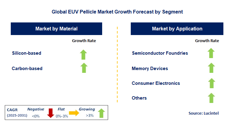
• Lucintel forecasts that, within the material category, carbon-based is expected to witness higher growth over the forecast period.
• Within the application category, semiconductor foundry, memory device, and consumer electronic is expected to witness the highest growth.
• In terms of region, APAC is expected to witness the highest growth over the forecast period. Gain valuable insights for your business decisions with our comprehensive 150+ page report. Sample figures with some insights are shown below.
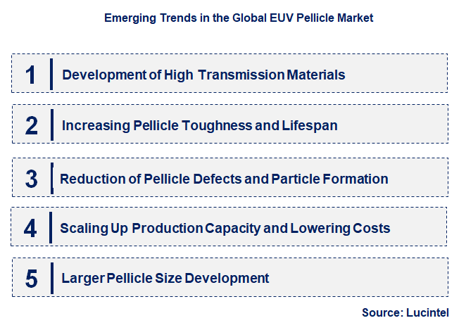
• Development of High Transmission Materials: Of supreme importance is the constant seeking for materials possessing drastically higher transmission performance at EUV wavelengths (close to 13.5 nm). Traditional pellicles manufactured from polysilicon or amorphous silicon are inherent to transmission restraints. Materials researchers are turned on to fresh avenues such as single layer graphene, carbon nanotubes, and ultra-thin metal films seeking to cut the absorption of and scattering from incident photons for further enhancing the lithographic processing efficacy and capacity.
• Increasing Pellicle Toughness and Lifespan: EUV lithography equipment employs high power light sources, which place extreme thermal and radiation stress on the pellicles. One of the trends is to create tougher pellicles that can withstand these harsh conditions for longer durations without compromising transmission or mechanical strength. This includes innovations in material composition, stress engineering, and protective coatings to increase pellicle lifespan and lower replacement frequency.
• Reduction of Pellicle Defects and Particle Formation: Any particle or defect on the pellicle can be transferred to the wafer, resulting in fatal errors in the process of semiconductor device manufacturing. One of the top trends is the use of sophisticated manufacturing processes and stringent quality control practices to reduce the initial defect density of EUV pellicles and avoid particle formation during usage. These include enhanced film deposition, handling, and packaging processes.
• Scaling Up Production Capacity and Lowering Costs: As EUV lithography enters mainstream high volume production, there is a growing necessity to scale up the production capacity of high quality EUV pellicles while reducing their cost at the same time. This trend requires the establishment of effective and scalable manufacturing processes, optimized supply chains, and greater competition among pellicle suppliers to provide the increased demand at an economically acceptable price for semiconductor manufacturers.
• Larger Pellicle Size Development: The industry trend towards bigger wafer sizes in semiconductor manufacturing requires the development of EUV pellicles with similarly bigger sizes. Producing large area, defect-free, and evenly thin membranes with high transmission and endurance is a major technical challenge. Current research and development efforts target overcoming these challenges to facilitate the implementation of larger pellicles in cutting-edge EUV lithography equipment. These trends are collectively redefining the EUV pellicle market by driving material science, manufacturing accuracy, and operational dependability to new heights. The developments in high transmission materials, high durability, defect reduction, scalable production, and bigger sizes are vital for the future success and economic attractiveness of EUV lithography as the foundation for subsequent semiconductor manufacturing.
• Improved Transmission Pellicles Commercialization: One of the major breakthroughs is progress towards EUV pellicles with better transmission than previous generations on the path towards commercialization. Though individual transmission rates differ, materials and thin film deposition technology advancements are resulting in pellicles that transmit greater amounts of EUV light, enhancing wafer throughputs and lowering the energy requirements for lithography tools.
• Greater Emphasis on Pellicle Metrology and Inspection: Since pellicle quality has a direct impact on wafer yield, there is greater emphasis on creating advanced metrology and inspection equipment for EUV pellicles. These consist of advanced methods for detecting and characterizing nanoscale defects, thickness uniformity measurements of films, and determination of transmission characteristics with high precision to ensure that only high-quality pellicles are utilized in production.
• Dual-Sided Pellicle Development: One new development is the investigation of dual sided pellicles, which would serve to shield both the mask and the optics from contamination. This idea has major technical challenges in terms of manufacturing and handling but might provide improved contamination control and possibly extend the life of critical EUV lithography components.
• Standardization Initiatives In the Supply Chain: With the maturation of the EUV ecosystem, there is a growing movement towards standardization of pellicle size, mounting interfaces, and performance characteristics. This standardization works towards enhanced interoperability, cost savings, and simplification of the supply chain for EUV pellicles, enabling them to be more widely adopted by semiconductor manufacturers.
• New Entrants in the Supply Chain: Although a handful of major players have controlled the initial EUV pellicle market, growing demand and prospects for innovation are encouraging new companies to enter the supply chain. These new entrants tend to concentrate on certain areas of pellicle technology, e.g., new materials or different manufacturing methods, which could bring more competition and a greater innovation rate. These advances are making a substantial contribution to the EUV pellicle market by overcoming key limitations associated with transmission, quality control, contamination management, and supply chain efficiency. These advances are necessary to make EUV lithography a more resilient and cost-effective technology for high volume production of advanced semiconductor devices.
• High Volume Manufacturing of Leading Edge Logic Devices: The dominant growth driver for the EUV pellicle market is the increasing application of EUV lithography for the production of leading edge logic semiconductors (such as next-generation CPUs, GPUs, and SoCs). With decreasing feature sizes, EUV becomes a requirement, calling for a guaranteed source of high performance pellicles to shield the costly and critical photomasks utilized in such processes.
• Fabrication of High-end DRAM and NAND Flash Memory: EUV lithography is also being widely embraced for fabrication of high-end Dynamic Random Access Memory (DRAM) and NAND flash memory chips. The challenging patterning demands for high-density memory devices find much benefit from the high-resolution capability of EUV, pushing the need for EUV pellicles into memory fabs.
• Increasing EUV Lithography to Additional Layers: Early on, EUV lithography was applied to a few select critical layers of semiconductor device manufacturing. As the technology continues to develop and pellicle performance gets better, the trend is toward applying EUV to more layers. The increased use of EUV per wafer immediately correlates to increased demand for EUV pellicles.
• Retrofitting existing EUV Lithography Tools: Already invested customers from semiconductor firms for EUV lithography equipment form a promising market for upgrade and replacement pellicles. As pellicle technology continuously evolves with more transmission and better lifetimes, there will also be a permanent possibility to retro-fit existing machines with these superior pellicles in order to improve productivity at lower operating cost.
• Future Applications in Advanced Packaging: Although presently targeting front end wafer processing, future developments in EUV lithography and pellicle technology may open up future applications in advanced packaging processes, which increasingly play a vital role in combining complex semiconductor devices. This might generate new opportunities for EUV pellicles in the long term. These strategic opportunities for growth, which are largely based on the growing use of EUV lithography in the production of next-generation logic and memory devices and its extension to additional layers, highlight the importance of EUV pellicles in making semiconductor technology's future possible. The necessity for these protective films will keep growing with the advancement and implementation of EUV lithography.
• ASML Holding
• Mitsui Chemicals
• Shin-Etsu Chemical
• FUJIFILM Holdings Corporation
• Toppan
• SÜSS MicroTec
• Entegris
• AGC
• Sumitomo Chemical
• SKC
• Silicon-based
• Carbon-based
• Semiconductor Foundries
• Memory Devices
• Consumer Electronics
• Others
• North America
• Europe
• Asia Pacific
• The Rest of the World
• United States: The United States is a key market for the EUV pellicle market, driven by dominant semiconductor leaders' demand and research institutions' contributions to material science development. Recent activity involves cooperation between industry and research labs to increase pellicle transmission and minimize defects. Robust pellicles that can handle the high power EUV light sources utilized in leading-edge lithography tools are also being developed.
• China: China's stake in the EUV pellicle market is expanding as it expands its plans in semiconductor fabrication. Current activity includes mounting investment in indigenous R&D of EUV-related technologies, including pellicles. Although it has technological challenges, Chinese companies are aggressively developing material and manufacturing process advancements to build a place in the supply chain for vital lithography parts.
• Germany: Germany is contributing to the EUV pellicle market with its significant presence in semiconductor manufacturing equipment and materials. Recent activity includes German companies contributing to the supply chain for EUV lithography tools, which indirectly fuels innovation and demand for high-quality pellicles. Research institutions are also contributing to materials science aspects pertinent to EUV pellicle development.
• India: Indian participation in the EUV pellicle market is presently restricted, given the fact that the country's semiconductor manufacturing facilities are still in the early stages of development. That said, growing government interest in establishing a local semiconductor ecosystem in the future may witness India emerge as a viable consumer and perhaps even a participant in the supply chain for EUV lithography equipment, including pellicles.
• Japan: Japan plays a prominent role in the EUV pellicle market, with major material suppliers and equipment makers playing active roles in the design and manufacture of these essential components. Recent advances include the development of ultra-thin membrane materials, improved manufacturing accuracy to reduce defects, and attempts to improve pellicle lifetime and thermal stability to address the high demands of high volume EUV lithography.

• ASML Holding
• Mitsui Chemicals
• Shin-Etsu Chemical
• FUJIFILM Holdings Corporation
• Toppan
• SÜSS MicroTec
• Entegris
• AGC
• Sumitomo Chemical
• SKC Q5. Which EUV pellicle market segment will be the largest in future? Answer: Lucintel forecasts that, within the material category, carbon-based is expected to witness higher growth over the forecast period. Q6. In EUV pellicle market, which region is expected to be the largest in next 5 years? Answer: In terms of region, APAC is expected to witness the highest growth over the forecast period. Q7. Do we receive customization in this report? Answer: Yes, Lucintel provides 10% customization without any additional cost.


Choose a license that fits your team. Instant PDF delivery.
Prices exclude taxes. Instant delivery. Custom licensing available on request.
Market Report · July 20, 2026
Market Report · July 16, 2026
Market Report · July 15, 2026
Trusted partner for strategic intelligence and business growth


Receive a complimentary market analysis tailored to your industry. Our analysts will identify key growth opportunities and competitive dynamics specific to your business.

Market size, growth rate, and key trend analysis for your specific sector.

Top competitor positioning and market share analysis.

Strategic recommendations backed by data-driven insights.
Get curated market intelligence and competitive moves straight to your inbox.
By subscribing, you agree to receive our monthly insights. Unsubscribe anytime.
Receive a complimentary market analysis tailored to your industry. Our analysts will identify key growth opportunities and competitive dynamics specific to your business.
Market size, growth rate, and key trend analysis for your specific sector.
Top competitor positioning and market share analysis.
Strategic recommendations backed by data-driven insights.
Get curated market intelligence, emerging trends, and competitive moves straight to your inbox each month.
By subscribing, you agree to receive our monthly insights. Unsubscribe anytime.
We'll send your sample report shortly.