
Market Report · July 29, 2026

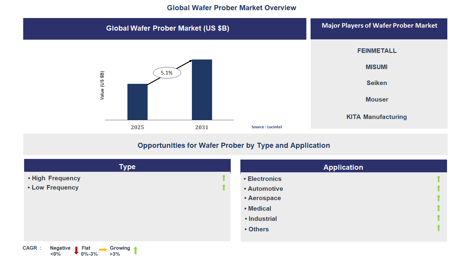
Key data points: The growth forecast = 5.1% annually for the next 7 years. Scroll below to get more insights. This market report covers trends, opportunities and forecasts in wafer prober market to 2031 by type (high frequency and low frequency), application (electronics, automotive, aerospace, medical, industrial, and others), and region (North America, Europe, Asia Pacific, and the Rest of the World)
We'll send your sample report shortly.
• Lucintel forecasts that, within the type category, high frequency is expected to witness higher growth over the forecast period.
• Within the application category, electronics is expected to witness the highest growth.
• In terms of region, APAC is expected to witness the highest growth over the forecast period. Gain valuable insights for your business decisions with our comprehensive 150+ page report. Sample figures with some insights are shown below.
• Integration of AI and Machine Learning: AI and machine learning algorithms are increasingly being integrated into wafer probers to improve accuracy and efficiency. These technologies enable real-time defect detection, predictive maintenance, and performance optimization. As AI becomes more advanced, it will enhance the diagnostic capabilities of probers, allowing for more reliable testing of high-performance chips.
• Miniaturization of Probing Systems: As semiconductor devices become smaller and more powerful, wafer probers are evolving to handle increasingly compact designs. Miniaturization trends are leading to the development of more compact, yet powerful, testing systems that can probe smaller chips without compromising on accuracy. This trend is essential for meeting the demands of modern electronics.
• Automation and Robotics Integration: Automation is a major trend in the wafer prober market, with robotics being increasingly integrated into wafer probing systems. This trend reduces human intervention, increasing throughput and consistency. Automated wafer probers can handle high-volume production runs with minimal downtime, improving the overall cost-effectiveness and scalability of semiconductor testing.
• Shift Toward Multi-Domain Applications: Wafer probers are becoming more versatile, with applications extending beyond traditional semiconductor testing to include automotive, medical, and aerospace sectors. This shift is driven by the growing need for high-precision testing in multiple industries that rely on semiconductors, such as autonomous vehicles, medical devices, and smart devices.
• Sustainability and Energy Efficiency: With increasing environmental concerns, the wafer prober market is witnessing a focus on sustainability. Manufacturers are designing energy-efficient and eco-friendly probers to minimize their environmental impact. Innovations include reducing energy consumption during the testing process and using sustainable materials for the construction of probing systems. These emerging trends—AI integration, miniaturization, automation, multi-domain applications, and sustainability—are revolutionizing the wafer prober market. They are driving more precise, efficient, and scalable solutions to meet the increasing demands of the semiconductor and electronics industries.

• Development of High-Precision Wafer Probers: Advances in precision technology have led to the creation of wafer probers capable of handling more intricate semiconductor designs. These probers offer higher resolution and sensitivity, allowing for more accurate testing of next-generation chips. This is particularly critical as semiconductor designs become more complex and demand increasingly higher standards of performance.
• Automation and Remote Operation Features: Many wafer probers are being equipped with enhanced automation and remote operation features. Automation enables faster testing, reduces human error, and improves consistency across production runs. Remote operation capabilities allow for reduced downtime and the ability to monitor the testing process from anywhere, making it more flexible and efficient.
• Advanced Materials for Probing Systems: Manufacturers are focusing on the development of advanced materials to improve the durability and efficiency of wafer probers. Materials that offer better resistance to wear and tear, as well as those that allow for higher thermal conductivity, are being integrated into probing systems to improve their performance in high-temperature environments.
• Integration of Multi-Functional Probing Systems: New wafer probers are being designed to perform a wider range of tasks, including electrical and thermal testing, to meet the growing needs of semiconductor testing. This multi-functional approach reduces the need for multiple machines, saving space and cost while improving the overall testing process.
• Emerging Nanotechnology in Wafer Probing: The integration of nanotechnology in wafer probers is becoming more common, allowing for the testing of even smaller devices with greater accuracy. Nanotechnology enables the creation of probes capable of measuring the properties of nanoscale semiconductors, crucial for the development of future generations of microelectronics. These developments—high-precision probers, automation, advanced materials, multi-functional systems, and nanotechnology—are enhancing the performance and capabilities of wafer probers. These innovations enable the testing of next-generation semiconductors and support the ongoing advancements in semiconductor and electronics industries.
• Expansion in Emerging Semiconductor Markets: As countries like India, Vietnam, and Brazil ramp up their semiconductor production capabilities, the demand for wafer probers is expected to grow. Manufacturers can tap into these emerging markets by offering affordable, yet high-quality, wafer testing systems tailored to local production needs.
• Integration with AI and IoT for Predictive Maintenance: Offering wafer probers integrated with AI and IoT technologies for predictive maintenance is a significant growth opportunity. These systems can predict equipment failure before it happens, reducing downtime and improving productivity. This predictive capability is essential in maintaining high throughput in semiconductor manufacturing.
• Focus on Energy-Efficient Probers: With the growing emphasis on sustainability, there is a strong market opportunity for energy-efficient wafer probers. Manufacturers can focus on developing low-energy systems that reduce the carbon footprint of semiconductor testing while maintaining high performance.
• Diversification into New Industry Verticals: The increasing demand for semiconductors in industries like automotive, healthcare, and aerospace opens up new opportunities for wafer probers. Manufacturers can explore diversification into these industries by developing specialized wafer probers for applications such as autonomous vehicles, medical devices, and industrial automation systems.
• Collaborations with Semiconductor Foundries: Building partnerships with semiconductor foundries to develop customized wafer probers is a strategic growth opportunity. Foundries often require highly specialized testing equipment for their advanced manufacturing processes, and collaborating with them can provide tailored solutions that meet their specific needs. These strategic growth opportunities—expansion in emerging markets, AI/IoT integration, energy-efficient systems, industry diversification, and collaborations with semiconductor foundries—are shaping the future of the wafer prober market. By addressing these areas, manufacturers can capitalize on the growing demand for advanced semiconductor testing solutions.
• FEINMETALL
• MISUMI
• Seiken
• Mouser
• KITA Manufacturing
• TOTOKU ELECTRIC
• Harwin
• Smiths Interconnect
• Sonel
• Leeno Industrial
• High Frequency
• Low Frequency
• Electronics
• Automotive
• Aerospace
• Medical
• Industrial
• Others
• North America
• Europe
• Asia Pacific
• The Rest of the World
• United States: The U.S. wafer prober market is witnessing innovations in automation and testing capabilities, particularly in the semiconductor industry. With the increasing demand for smaller devices and cutting-edge chips, companies are investing in advanced probing technologies. Automation in wafer probing processes is improving efficiency and accuracy, which is crucial for meeting the growing performance requirements of semiconductor devices.
• China: Chinas wafer prober market is expanding rapidly as the country ramps up its semiconductor production capabilities. The focus is on increasing local manufacturing of probing systems to reduce reliance on foreign imports. Chinese manufacturers are developing cost-effective probing systems that meet the needs of its burgeoning electronics industry, particularly for mobile devices, consumer electronics, and industrial applications.
• Germany: Germany remains a leader in precision manufacturing, and its wafer prober market is benefiting from the country’s strong focus on automation and quality control. The demand for advanced probes in automotive and industrial electronics has spurred growth. German manufacturers are integrating Industry 4.0 concepts to improve efficiency and precision, while focusing on sustainability and eco-friendly materials in their probe designs.
• India: In India, the wafer prober market is emerging as the country invests more in semiconductor production and electronics manufacturing. While still in its growth phase, India’s wafer prober market is seeing increasing demand from the local electronics and consumer goods industries. With government incentives and growing tech investments, India is gradually becoming a hub for semiconductor testing equipment.
• Japan: Japan’s wafer prober market is characterized by high precision and innovation, supported by its robust semiconductor industry. Japanese manufacturers are leading in the development of advanced wafer probers used for both mass production and research applications. The focus is on increasing automation and improving the accuracy of testing processes, which is crucial for maintaining Japan’s competitive edge in semiconductor technology.


• FEINMETALL
• MISUMI
• Seiken
• Mouser
• KITA Manufacturing
• TOTOKU ELECTRIC
• Harwin
• Smiths Interconnect
• Sonel
• Leeno Industrial Q5. Which wafer prober market segment will be the largest in future? Answer: Lucintel forecasts that, within the type category, high frequency is expected to witness higher growth over the forecast period. Q6. In wafer prober market, which region is expected to be the largest in next 5 years? Answer: In terms of region, APAC is expected to witness the highest growth over the forecast period. Q7. Do we receive customization in this report? Answer: Yes, Lucintel provides 10% customization without any additional cost.


Choose a license that fits your team. Instant PDF delivery.
Prices exclude taxes. Instant delivery. Custom licensing available on request.
Market Report · July 29, 2026
Market Report · July 20, 2026
Market Report · July 20, 2026
Trusted partner for strategic intelligence and business growth


Receive a complimentary market analysis tailored to your industry. Our analysts will identify key growth opportunities and competitive dynamics specific to your business.

Market size, growth rate, and key trend analysis for your specific sector.

Top competitor positioning and market share analysis.

Strategic recommendations backed by data-driven insights.
Get curated market intelligence and competitive moves straight to your inbox.
By subscribing, you agree to receive our monthly insights. Unsubscribe anytime.
Receive a complimentary market analysis tailored to your industry. Our analysts will identify key growth opportunities and competitive dynamics specific to your business.
Market size, growth rate, and key trend analysis for your specific sector.
Top competitor positioning and market share analysis.
Strategic recommendations backed by data-driven insights.
Get curated market intelligence, emerging trends, and competitive moves straight to your inbox each month.
By subscribing, you agree to receive our monthly insights. Unsubscribe anytime.
We'll send your sample report shortly.