
Wafer Bump Processing Service Market Report: Trends, Forecast and Competitive Analysis to 2035

Key data points: The market size in 2035 = $7 billion, growth forecast = 6.5% annually for the next 8 years. Scroll below to get more insights. This market report covers trends, opportunities and forecasts in wafer bump processing service market to 2035 by type (copper pillar bumping, solder bumping, and gold bumping), application (200mm wafer and 300mm wafer), and region (North America, Europe, Asia Pacific, and the Rest of the World)

Publisher: Lucintel Last Updated: July 2026
See Pricing

Download Sample Report

| ✨ New Download Sample report — Get instant insights! | ✨ New Download Sample report — Get instant insights!

Wafer Bump Processing Service Market Report: Trends, Forecast and Competitive Analysis to 2035

Wafer Bump Processing Service Market

The future of the global wafer bump processing service market looks promising with opportunities in the copper pillar bumping, solder bumping, and gold bumping markets. The global wafer bump processing service market is expected to reach an estimated $7 billion by 2035 with a CAGR of 6.5% from 2026 to 2035. The major drivers for this market are the increasing demand for advanced chip packaging, the rising adoption of semiconductor miniaturization technologies, and the growing use of high density wafer interconnect solutions.

  • Lucintel forecasts that, within the application category, 300mm wafer is expected to witness higher growth over the forecast period due to the increasing demand for advanced semiconductor manufacturing processes.
  • Within the type category, copper pillar bumping is expected to witness the highest growth due to the growing adoption of high-performance chip packaging technologies.
  • In terms of regions, APAC is expected to witness the highest growth over the forecast period due to the rising semiconductor production and electronics industry expansion.

Gain valuable insights for your business decisions with our comprehensive 150+ page report. Sample figures with some insights are shown below.
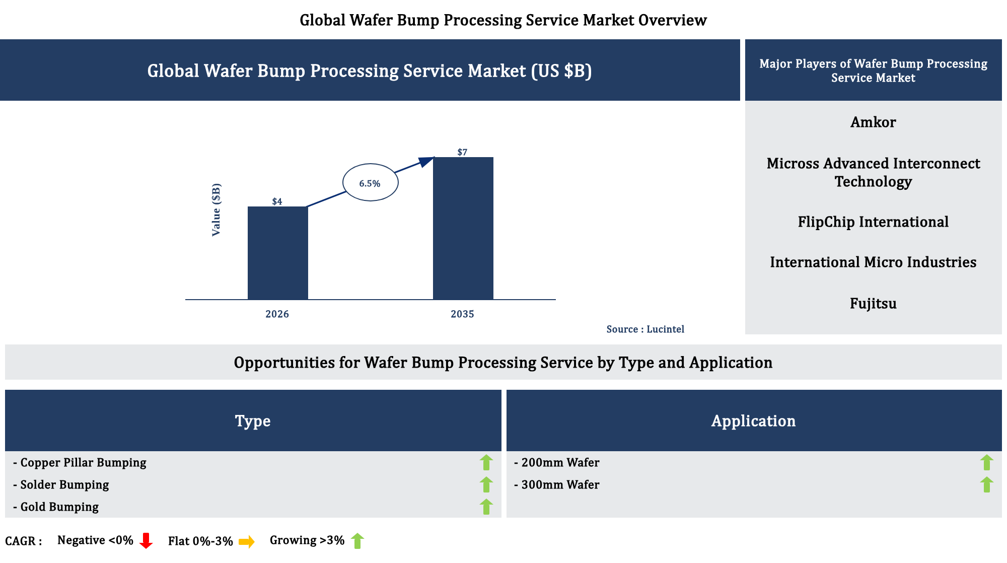
Wafer Bump Processing Service Market

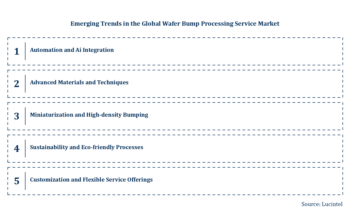
Emerging Trends in the Wafer Bump Processing Service Market

The wafer bump processing service market is experiencing rapid evolution driven by technological advancements, increasing demand for miniaturized electronic devices, and the need for higher precision in semiconductor manufacturing. As the electronics industry pushes towards smaller, more powerful, and energy-efficient devices, the market is adapting to meet these demands through innovative processes and materials. Emerging trends are shaping the competitive landscape, influencing supply chains, and fostering new opportunities for service providers. These developments are not only enhancing product performance but also reducing costs and lead times, ultimately transforming the way semiconductor components are manufactured and integrated into various electronic applications.

  • Automation and AI Integration: The adoption of automation and artificial intelligence in wafer bump processing is streamlining operations, reducing human error, and increasing throughput. AI-driven quality control systems enable real-time defect detection, ensuring higher yield rates. This trend enhances efficiency, lowers operational costs, and accelerates production cycles, making advanced wafer bumping more accessible and reliable for manufacturers.
  • Advanced Materials and Techniques: The shift towards using novel materials such as copper, tin, and lead-free alloys in bumping processes improves electrical performance and environmental compliance. Techniques like micro-bumping and through-silicon via (TSV) bumping are gaining prominence, enabling higher density interconnects and better thermal management. These innovations support the development of 3D integrated circuits and high-performance devices.
  • Miniaturization and High-Density Bumping: As devices become smaller and more powerful, the demand for high-density bumping solutions increases. Fine-pitch and ultra-fine bumping techniques are being adopted to accommodate the shrinking geometries of chips. This trend allows for more compact devices with enhanced functionality, catering to markets such as smartphones, wearables, and IoT devices.
  • Sustainability and Eco-Friendly Processes: Environmental concerns are prompting the industry to adopt greener bumping processes, such as lead-free soldering and waste reduction practices. Companies are investing in sustainable materials and recycling methods to minimize ecological impact. This shift not only aligns with regulatory standards but also appeals to environmentally conscious consumers and clients.
  • Customization and Flexible Service Offerings: The market is witnessing a move towards tailored wafer bumping solutions to meet specific client requirements. Service providers are offering flexible processing options, including different bump sizes, pitches, and materials, to cater to diverse applications. This customization enhances customer satisfaction and opens new avenues for niche markets like automotive and aerospace electronics.

These emerging trends are significantly reshaping the wafer bump processing service market by fostering innovation, improving efficiency, and emphasizing sustainability. They enable manufacturers to produce smaller, more powerful, and environmentally friendly electronic devices, thereby driving growth and competitiveness in the semiconductor industry.
Wafer Bump Processing Service Market by country

Recent Developments in the Wafer Bump Processing Service Market

The wafer bump processing service market is experiencing rapid growth driven by advancements in semiconductor manufacturing, increasing demand for high-performance electronics, and technological innovations. As the industry evolves, key developments are shaping the future landscape, offering new opportunities for manufacturers and service providers. These developments are crucial for enhancing product quality, reducing costs, and meeting the rising needs of various end-use sectors such as consumer electronics, automotive, and telecommunications.

  • Technological Innovations in Bump Materials: The adoption of advanced bump materials like copper, gold, and solder alloys is improving reliability and performance. These innovations enable finer pitch and smaller bump sizes, essential for miniaturization. Enhanced material properties reduce defects and improve electrical conductivity, leading to higher yields. This development is attracting more semiconductor manufacturers to adopt wafer bumping services, thereby expanding market reach and driving growth.
  • Automation and AI Integration in Bumping Processes: The integration of automation and artificial intelligence (AI) is streamlining wafer bumping processes, increasing precision, and reducing human error. Automated systems enable faster processing times and consistent quality, which are critical for high-volume production. AI-driven defect detection and process optimization further enhance yield rates. This technological leap is making wafer bumping more cost-effective and scalable, attracting new players and boosting overall market competitiveness.
  • Expansion of Service Offerings with Advanced Packaging: Service providers are now offering comprehensive advanced packaging solutions, including 2.5D and 3D IC packaging. These offerings support higher interconnect density and improved performance for complex semiconductor devices. The ability to provide end-to-end solutions from bumping to final packaging is attracting clients seeking integrated services. This expansion is fostering innovation and increasing the market size by catering to diverse application needs.
  • Growing Demand from Emerging Markets: Rapid industrialization and technological adoption in emerging markets like China, India, and Southeast Asia are fueling demand for wafer bumping services. These regions are witnessing increased investments in semiconductor manufacturing facilities. Localized service providers are expanding capacities to meet regional needs, reducing reliance on imports. This growth is diversifying the market landscape and creating new opportunities for global and regional players.
  • Sustainability and Eco-Friendly Bumping Solutions: The industry is shifting towards environmentally sustainable bumping processes, including the use of lead-free materials and waste reduction techniques. These eco-friendly solutions comply with global regulations and appeal to environmentally conscious consumers. Adoption of green practices is also reducing operational costs and enhancing brand reputation. This development is driving innovation in materials and processes, positioning the market as more sustainable and future-ready.

These recent developments are significantly transforming the wafer bump processing service market by enhancing technological capabilities, expanding service offerings, and entering new regional markets. The focus on innovation, automation, and sustainability is increasing efficiency, reducing costs, and meeting evolving customer demands. As a result, the market is poised for sustained growth, attracting investments and fostering competitive advantages for industry players worldwide.

Strategic Growth Opportunities in the Wafer Bump Processing Service Market

The wafer bump processing service market is experiencing rapid expansion driven by advancements in semiconductor manufacturing, increasing demand for miniaturized electronic devices, and the need for high-precision packaging solutions. Innovations in bumping technologies and the rise of 5G, IoT, and automotive electronics are fueling growth. Market players are focusing on enhancing process efficiency, reducing costs, and expanding service offerings to meet diverse customer needs across various applications and regions, creating significant opportunities for strategic development.

  • Technological Advancements in Bumping Techniques: The adoption of advanced bumping methods such as copper pillar, micro-bump, and hybrid bumping is expanding the market. These innovations improve electrical performance, reliability, and miniaturization, catering to high-performance applications like 5G devices, AI chips, and high-speed computing. As companies invest in R&D, the availability of diverse bumping options enhances customization, driving growth in high-end semiconductor packaging services.
  • Growing Demand for 3D IC and Advanced Packaging: The increasing adoption of 3D integrated circuits and advanced packaging solutions creates substantial opportunities for wafer bump processing services. These technologies enable higher device density, improved performance, and reduced form factors, essential for smartphones, data centers, and automotive electronics. Service providers focusing on fine-pitch bumping and through-silicon via (TSV) processes are positioned to capitalize on this trend.
  • Expansion of Semiconductor Manufacturing in Emerging Markets: Countries like China, India, and Southeast Asian nations are investing heavily in semiconductor fabrication facilities. This regional growth boosts demand for wafer bump processing services, especially for local chip manufacturers seeking cost-effective and reliable solutions. Strategic partnerships and localized service centers are key to capturing market share in these emerging regions.
  • Integration of Automation and AI in Bumping Processes: Automation and artificial intelligence are transforming wafer bump processing by enhancing precision, reducing defects, and increasing throughput. Automated inspection, defect detection, and process optimization improve yield rates and cost efficiency. Companies adopting these technologies can offer faster turnaround times and higher quality services, gaining a competitive edge in a highly technical market.
  • Diversification of Service Offerings for Different Applications: The market is witnessing a shift towards specialized bumping services tailored for specific applications such as automotive, IoT, and consumer electronics. Custom solutions like flip-chip, wafer-level packaging, and fan-out wafer-level packaging are expanding the service portfolio. This diversification allows providers to meet the unique requirements of various end-use sectors, fostering long-term customer relationships and market growth.

These strategic growth opportunities are poised to significantly influence the wafer bump processing service market by fostering innovation, expanding regional presence, and diversifying service offerings. Embracing technological advancements and addressing emerging application needs will enable market players to strengthen their competitive position. Overall, these opportunities will drive sustained growth, improve service quality, and meet the evolving demands of the semiconductor industry worldwide.

Wafer Bump Processing Service Market Drivers and Challenges

The wafer bump processing service market is influenced by a variety of technological, economic, and regulatory factors that shape its growth and development. Rapid advancements in semiconductor technology demand more precise and efficient bump processing solutions, while economic fluctuations impact investment and operational costs. Regulatory standards concerning environmental safety and quality assurance also play a crucial role in shaping industry practices. Additionally, global supply chain dynamics and geopolitical considerations influence market stability and expansion opportunities. Understanding these drivers and challenges is essential for stakeholders to navigate the evolving landscape and capitalize on emerging trends effectively.

The factors responsible for driving the wafer bump processing service market include:-

  • Technological Innovation: The continuous evolution of semiconductor devices necessitates advanced bump processing techniques, such as fine-pitch bumping and 3D integration, which enhance device performance and miniaturization. Innovations in materials and process automation improve efficiency, reduce defects, and lower costs, fueling market growth. As demand for high-performance electronics increases, the need for sophisticated bump processing solutions becomes critical, driving investments and R&D activities in this sector.
  • Growing Semiconductor Demand: The expanding use of semiconductors across industries like consumer electronics, automotive, and healthcare significantly boosts the demand for wafer bump processing services. The proliferation of IoT devices, 5G infrastructure, and electric vehicles requires high-volume, reliable bumping solutions, prompting manufacturers to outsource these services to specialized providers, thereby expanding the market.
  • Miniaturization and Complexity: The trend toward smaller, more complex semiconductor devices demands precise bumping techniques capable of handling ultra-fine pitches and multi-layered structures. This complexity drives the adoption of advanced bump processing services that can meet stringent quality and performance standards, fostering market growth as manufacturers seek to stay competitive.
  • Environmental and Regulatory Standards: Increasing regulatory requirements related to environmental safety, waste management, and product quality influence bump processing practices. Companies investing in eco-friendly materials and processes to comply with regulations gain a competitive edge, encouraging innovation and sustainable practices within the industry.

The challenges facing the wafer bump processing service market are:-

  • High Capital Investment: Establishing advanced bump processing facilities requires significant capital expenditure on equipment, technology, and skilled personnel. This high initial investment can be a barrier for new entrants and limit expansion for existing players, especially in regions with limited financial resources, impacting overall market growth.
  • Technological Complexity and Rapid Obsolescence: The fast-paced nature of technological advancements leads to frequent updates in bumping techniques and materials. Keeping pace with these changes demands continuous R&D investment, which can be costly and challenging for companies to sustain, potentially causing delays and increased operational risks.
  • Supply Chain Disruptions: The global semiconductor supply chain is vulnerable to disruptions caused by geopolitical tensions, pandemics, and logistical issues. These disruptions can lead to shortages of raw materials and equipment, delays in production schedules, and increased costs, adversely affecting the efficiency and profitability of bump processing service providers.

The wafer bump processing service market is driven by technological innovation, rising semiconductor demand, miniaturization trends, and regulatory compliance. However, high capital costs, rapid technological changes, and supply chain vulnerabilities pose significant challenges. These factors collectively influence market dynamics, requiring stakeholders to adapt strategically to sustain growth and competitiveness in a rapidly evolving industry landscape.

List of Wafer Bump Processing Service Market Companies

Companies in the market compete on the basis of product quality offered. Major players in this market focus on expanding their manufacturing facilities, R&D investments, infrastructural development, and leverage integration opportunities across the value chain. Through these strategies wafer bump processing service market companies cater increasing demand, ensure competitive effectiveness, develop innovative products & technologies, reduce production costs, and expand their customer base. Some of the wafer bump processing service market companies profiled in this report include-

  • Amkor
  • Micross Advanced Interconnect Technology
  • FlipChip International
  • International Micro Industries
  • Fujitsu
  • ASE Global
  • Nepes
  • Maxell
  • Chipmore Technology
  • ChipMOS

Wafer Bump Processing Service Market by Segment

The study includes a forecast for the global wafer bump processing service market by type, application, and region.

  • Wafer Bump Processing Service Market by Type [Value from 2019 to 2035]:
    • Copper Pillar Bumping
    • Solder Bumping
    • Gold Bumping
  • Wafer Bump Processing Service Market by Application [Value from 2019 to 2035]:
    • 200mm Wafer
    • 300mm Wafer
  • Wafer Bump Processing Service Market by Region [Value ($B) from 2019 to 2035]:
    • North America
    • Europe
    • Asia Pacific
    • The Rest of the World

Country Wise Outlook for the Wafer Bump Processing Service Market

The wafer bump processing service market has experienced significant technological advancements and shifts in demand driven by the semiconductor industry's rapid growth. As the industry evolves, countries are investing heavily in innovation, infrastructure, and capacity expansion to meet the increasing need for high-performance electronic devices. These developments are crucial for enhancing chip performance, reducing costs, and supporting emerging technologies such as AI, 5G, and IoT. The competitive landscape is also changing, with new players entering the market and existing ones upgrading their capabilities to maintain their market share. Here is a country-specific overview of recent developments in this market.

  • United States: The United States has seen substantial investments in advanced wafer bumping technologies, including the adoption of ultra-fine pitch bumping and lead-free processes. Major players are focusing on automation and quality control to improve yield rates. The U.S. government is also supporting R&D initiatives to develop next-generation packaging solutions, fostering innovation in the semiconductor supply chain. Additionally, collaborations between tech giants and startups are accelerating the deployment of innovative bumping techniques.
  • China: China continues to expand its manufacturing capacity for wafer bumping services, driven by government policies aimed at reducing reliance on foreign technology. The country is investing in advanced equipment and training skilled personnel to enhance its technological capabilities. Chinese firms are increasingly adopting advanced bumping processes such as copper pillar and flip-chip bumping to cater to the growing demand for high-density packaging. Strategic partnerships with international equipment suppliers are also strengthening China's position in this market.
  • Germany: Germany remains a key player in the European semiconductor ecosystem, focusing on high-precision wafer bumping for automotive and industrial applications. Recent developments include the integration of AI-driven inspection systems to improve defect detection and process control. German companies are also investing in sustainable manufacturing practices, reducing environmental impact. The country is fostering collaborations between research institutions and industry to develop innovative bumping materials and techniques, maintaining its competitive edge.
  • India: India is rapidly emerging as a significant hub for wafer bump processing, supported by government initiatives like Make in India and Digital India. The country is witnessing increased investments in semiconductor manufacturing facilities and R&D centers. Indian firms are adopting advanced bumping technologies such as micro-bump and copper pillar bumping to meet domestic and export demands. The focus is also on skill development and technology transfer to build a robust semiconductor ecosystem capable of competing globally.
  • Japan: Japan continues to innovate in wafer bump processing, emphasizing reliability and miniaturization. Recent advancements include the development of new bumping materials that enhance thermal and electrical performance. Japanese companies are also exploring flexible and stretchable bumping solutions for emerging applications like wearable electronics. The country is investing in automation and precision equipment to improve process efficiency and yield. Collaborations with international firms are facilitating the transfer of cutting-edge technologies, ensuring Japan's leadership in high-quality wafer bumping services.

Features of the Wafer Bump Processing Service Market

  • Market Size Estimates: Wafer bump processing service market size estimation in terms of value ($B).
  • Trend and Forecast Analysis: Market trends (2019 to 2025) and forecast (2026 to 2035) by various segments and regions.
  • Segmentation Analysis: Wafer bump processing service market size by type, application, and region in terms of value ($B).
  • Regional Analysis: Wafer bump processing service market breakdown by North America, Europe, Asia Pacific, and Rest of the World.
  • Growth Opportunities: Analysis of growth opportunities in different types, applications, and regions for the wafer bump processing service market.
  • Strategic Analysis: This includes M&A, new product development, and competitive landscape of the wafer bump processing service market.
  • Analysis of competitive intensity of the industry based on Porter’s Five Forces model.

Top 5 Companies

  • Amkor
  • Micross Advanced Interconnect Technology
  • FlipChip International
  • International Micro Industries
  • Fujitsu

Table of Contents

1. Executive Summary
13.1 Competitive Analysis Overview

List of Figures

List of Tables

Methodology

Lucintel has been in the business of market research and management consulting since 2000 and has published over 1000 market intelligence reports in various markets / applications and served over 1,000 clients worldwide. This study is a culmination of four months of full-time effort performed by Lucintel's analyst team. The analysts used the following sources for the creation and completion of this valuable report:

  • In-depth interviews of the major players in this market
  • Detailed secondary research from competitors' financial statements and published data
  • Extensive searches of published works, market, and database information pertaining to industry news, company press releases, and customer intentions
  • A compilation of the experiences, judgments, and insights of Lucintel's professionals, who have analyzed and tracked this market over the years.

Extensive research and interviews are conducted across the supply chain of this market to estimate market share, market size, trends, drivers, challenges, and forecasts. Below is a brief summary of the primary interviews that were conducted by job function for this report.

Lucintel's methodology for market research

Thus, Lucintel compiles vast amounts of data from numerous sources, validates the integrity of that data, and performs a comprehensive analysis. Lucintel then organizes the data, its findings, and insights into a concise report designed to support the strategic decision-making process. The figure below is a graphical representation of Lucintel's research process.

Primary interviews by job function

Buy Now

Choose a license that fits your team. Instant PDF delivery.

Market Report

1 User PDF

$4,850
Buy Now

Market Report

2-5 Users PDF

$6,700
Buy Now

Market Report

Corporate PDF

$8,850
Buy Now

Market Report

Global PDF

$10,000
Buy Now

Prices exclude taxes. Instant delivery. Custom licensing available on request.

Frequently Asked Questions

What is the wafer bump processing service market size?
The global wafer bump processing service market is expected to reach an estimated $7 billion by 2035.
What is the growth forecast for wafer bump processing service market?
The global wafer bump processing service market is expected to grow with a CAGR of 6.5% from 2026 to 2035.
What are the major drivers influencing the growth of the wafer bump processing service market?
The major drivers for this market are the increasing demand for advanced chip packaging, the rising adoption of semiconductor miniaturization technologies, and the growing use of high density wafer interconnect solutions.
What are the major segments for wafer bump processing service market?
The future of the wafer bump processing service market looks promising with opportunities in the copper pillar bumping, solder bumping, and gold bumping markets.
Who are the key wafer bump processing service market companies?

Some of the key wafer bump processing service companies are as follows:

  • Amkor
  • Micross Advanced Interconnect Technology
  • FlipChip International
  • International Micro Industries
  • Fujitsu
  • ASE Global
  • Nepes
  • Maxell
  • Chipmore Technology
  • ChipMOS
Which wafer bump processing service market segment will be the largest in future?
Lucintel forecasts that, within the application category, 300mm wafer is expected to witness higher growth over the forecast period.
In wafer bump processing service market, which region is expected to be the largest in next 8 years?
In terms of region, APAC is expected to witness the highest growth over the forecast period.
Do we receive customization in this report?
Yes, Lucintel provides 10% customization without any additional cost.

Key Questions

  • What are some of the most promising, high-growth opportunities for the wafer bump processing service market by type (copper pillar bumping, solder bumping, and gold bumping), application (200mm wafer and 300mm wafer), and region (North America, Europe, Asia Pacific, and the Rest of the World)?
  • Which segments will grow at a faster pace and why?
  • Which region will grow at a faster pace and why?
  • What are the key factors affecting market dynamics? What are the key challenges and business risks in this market?
  • What are the business risks and competitive threats in this market?
  • What are the emerging trends in this market and the reasons behind them?
  • What are some of the changing demands of customers in the market?
  • What are the new developments in the market? Which companies are leading these developments?
  • Who are the major players in this market? What strategic initiatives are key players pursuing for business growth?
  • What are some of the competing products in this market and how big of a threat do they pose for loss of market share by material or product substitution?
  • What M&A activity has occurred in the last 5 years and what has its impact been on the industry?
Why Choose Us

The Lucintel Advantage

Trusted partner for strategic intelligence and business growth

25+ Years Excellence

25+ Years Excellence

Quarter century of proven expertise in management consulting and market research across global markets.
Game-Changer Ideas

Game-Changer Ideas

Innovative strategies and actionable insights that help clients become the smartest in their industry.
Global Reach

Global Reach

Extensive coverage across 50+ industries and markets worldwide with localized expertise.
Start Your Growth Journey

Get Your Free
Market Intelligence
Briefing

Receive a complimentary market analysis tailored to your industry. Our analysts will identify key growth opportunities and competitive dynamics specific to your business.

Custom Market Snapshot

Market size, growth rate, and key trend analysis for your specific sector.

Competitive Landscape Overview

Top competitor positioning and market share analysis.

Growth Opportunity Identification

Strategic recommendations backed by data-driven insights.

Subscribe

Subscribe to our Newsletter

Get curated market intelligence and competitive moves straight to your inbox.

By subscribing, you agree to receive our monthly insights. Unsubscribe anytime.

Industry Trends Market Signals Opportunities Competitor Moves