
Market Report · July 29, 2026

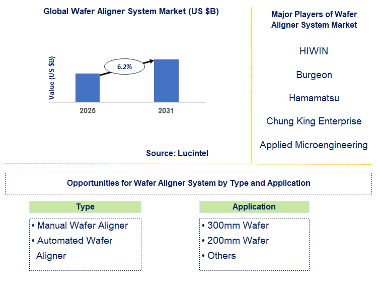
Key data points: The growth forecast = 6.2% annually for the next 7 years. Scroll below to get more insights. This market report covers trends, opportunities and forecasts in wafer aligner system market to 2031 by type (manual wafer aligner and automated wafer aligner), application (300mm wafer, 200mm wafer, and others), and region (North America, Europe, Asia Pacific, and the Rest of the World)
We'll send your sample report shortly.
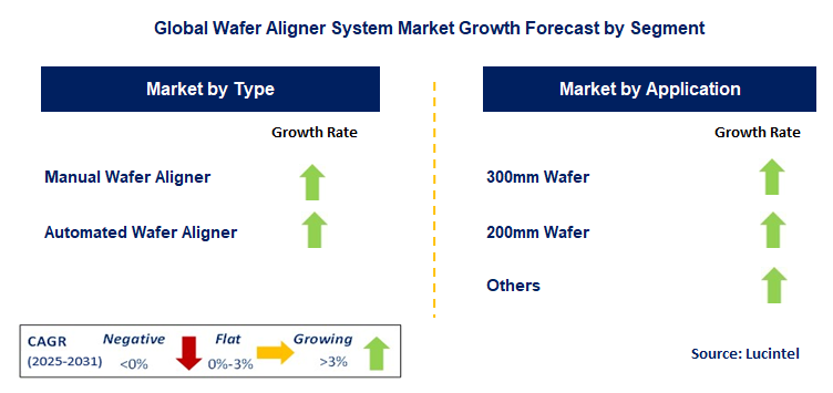
• Lucintel forecasts that, within the type category, automated wafer aligner is expected to witness higher growth over the forecast period.
• Within the application category, 300mm wafer is expected to witness higher growth.
• In terms of region, APAC is expected to witness the highest growth over the forecast period. Gain valuable insights for your business decisions with our comprehensive 150+ page report. Sample figures with some insights are shown below.
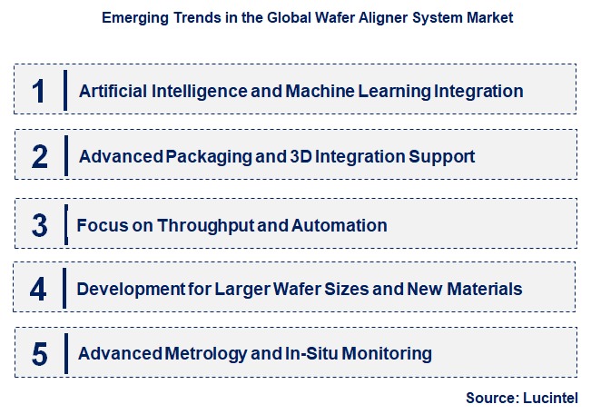
• Artificial Intelligence and Machine Learning Integration: This trend is about using AI and ML algorithms to improve the accuracy, speed, and overall efficiency of wafer alignment operations. AI is capable of processing complex metrology data, forecasting alignment drifts, and optimizing alignment routines in real time with minimal intervention by humans. The benefits include enhanced yield rates through reduced alignment errors, quicker cycle times for photolithography, and the capability to manage growing process variations in advanced nodes. This also aids in predictive maintenance, decreasing downtime and maximizing equipment usage.
• Advanced Packaging and 3D Integration Support: With 2D scaling becoming increasingly slow, advanced packaging methods such as 3D integration (stacking dies) and heterogeneous integration are becoming more prominent. Wafer aligner systems are adapting to supply extremely accurate alignment for wafer-to-wafer bonding and die-to-wafer bonding. The effect is facilitating the manufacturing of smaller, more powerful, and energy-efficient devices. Such a trend necessitates innovation towards new alignment modalities that can accommodate fragile thin wafers and intricate multi-layer structures necessary for the next generation of microelectronics.
• Focus on Throughput and Automation: Due to growing needs for semiconductor chips, there is a great emphasis on increasing the throughput of wafer aligners without compromising ultra-high accuracy. This entails the integration of higher-speed wafer handling robots, high-performance vision systems, and automated process control. The result is increased volumes of production and reduced manufacturing costs per chip. This trend is critical in high-volume manufacturing (HVM) settings where every second of processing time has a direct impact on profitability and supply to the marketplace.
• Development for Larger Wafer Sizes and New Materials: Although 300mm wafers are the norm, there is ongoing investigation into even larger wafers and the processing of new substrate materials (e.g., silicon carbide, gallium nitride) for target applications such as power electronics and optoelectronics. Wafer aligner systems are being made available to handle these larger sizes and the special characteristics of these materials. The effect is making economies of scale available to future semiconductor manufacturing and enabling the expansion of specialized semiconductor markets beyond the conventional silicon.
• Advanced Metrology and In-Situ Monitoring: The direction is putting more advanced in-situ metrology instruments and real-time monitoring directly into wafer aligner systems. This provides instant feedback on process deviations and alignment accuracy without requiring the wafer to be removed from the system. The effect is diminishing inspection time, allowing for quicker error correction, and enhancing yield further by guaranteeing the quality of alignment at each step of the process. This produces a more solid and responsive manufacturing environment. These are all converging to redefine the wafer aligner system market by stretching the envelope of precision and productivity. The use of smart technology, flexibility to adapt to emerging packaging paradigms, and constant drive for improved throughput are ensuring that wafer aligner systems are always critical components to the semiconductor industry's ongoing innovation.
• Sub-Nanometer Alignment Precision Obtained: One notable recent advancement is the attainment of sub-nanometer alignment accuracy in next-generation wafer aligner systems, going beyond micron or even nanometer levels. It is necessary for making chips at 3nm and below process nodes. The effect is to continue to miniaturize transistors and pack more devices onto one chip, which in turn directly benefits the performance increases of future processors, memory, and specialty semiconductors.
• Increased Automation and Integration with Robotics: There has been considerable advancement in automating handling and wafer alignment processes, where advanced robotics and vision systems are now the norm. Highly automated systems load, pre-align, and accurately align wafers with minimal manual intervention. The effect is greatly improving throughput, lowering labor expenses, and reducing human-caused errors and particle contamination in cleanroom conditions. This is critical for high-volume manufacturing (HVM) in contemporary fabrication plants.
• Optical and Vision Systems: Recent advances include the addition of more sophisticated optical recognition software and high-resolution imaging instruments to wafer aligners. These instruments can identify fine alignment marks on wafers, even on difficult or damaged surfaces, with higher speed and accuracy. The effect is increased alignment strength over varying wafer types and process variations, resulting in greater yield and less rework, which are essential for economical semiconductor manufacturing.
• Greater Compatibility with Next-Generation Packaging Technologies: Wafer aligner tools are actually being designed or repurposed specifically to address the specific needs of next-generation packaging methods like 3D stacking, chaplet packaging, and wafer-level packaging. This encompasses features for the alignment of very thin wafers or wafers possessing pre-existing through-silicon vias (TSVs). The effect is enabling the next generation of heterogeneous integration, where various chip functions are integrated into one small package, which accelerates innovation in consumer electronics, automotive, and high-performance computing.
• Real-Time Process Monitoring and Feedback Implementation: Contemporary wafer aligner systems are more and more integrating in-situ metrology and real-time feedback loops. This permits ongoing monitoring of the accuracy of alignment during processing and on-the-fly adjustments in case of deviations. The effect is active error correction, reducing scrap rates, and enhancing overall process control. This translates into increased manufacturing yields and enhanced consistency of chip quality, which are imperative to the competitive semiconductor industry. These latest advancements are all together influencing the wafer aligner system market by expanding the limits of precision, automation, and flexibility. The ongoing improvement of these systems is crucial for the semiconductor industry to reach its objectives of manufacturing more powerful, smaller, and affordable electronic devices.
• Next-Generation Logic and Memory Fabrication: Ongoing scaling of logic and memory chips into deep nodes (e.g., 3nm, 2nm) necessitates wafer aligner equipment with levels of accuracy and consistency unprecedented in the industry. This underlying imperative represents a leading-edge growth opportunity for suppliers that can provide next-generation alignment technology for these front-edge fab lines. The effect is a long-term demand for highly sophisticated and costly aligner systems by best-in-class foundries and integrated device manufacturers (IDMs), creating high-value market segments.
• Next-Generation Packaging and Heterogeneous Integration: The move toward next-generation packaging methods, such as 2.5D and 3D integration, wafer-level packaging, and chip let assembly, presents a unique growth opportunity. These techniques are highly dependent on ultra-accurate wafer-to-wafer or die-to-wafer alignment. The effect is a new market segment for aligner systems tailored to work with thin, fragile wafers and intricate multi-layered structures, allowing for more performance and reduced form factor in end-applications such as high-performance computing (HPC) and AI accelerators.
• Fabrication of MEMS, Sensors, and Power Devices: The increasing need for Micro-Electro-Mechanical Systems (MEMS), sensors (e.g., automotive, IoT), and power semiconductor devices (e.g., on Sic, Gan substrates) is a strong growth driver. Many of these applications demand niche alignment capabilities between various substrate materials and device structures. The effect is a diversified customer base for wafer aligner system makers, expanding beyond the legacy logic and memory, and demanding flexible systems in these niche, high-growth areas.
• Upcoming Semiconductor Manufacturing Hubs: Worldwide semiconductor manufacturing diversification, as new fabs emerge in countries such as India, Southeast Asia, and parts of Europe, presents important greenfield growth opportunities. The new facilities will demand a complete fabrication equipment package, including wafer aligner systems. The effect is the possibility of new market entry and heightened volume of sales, as incumbent and new producers grow their global presence, fueled by government support and supply chain resilience measures.
• Research and Development in Novel Lithography Techniques: Continued R&D in next-generation lithography methods, beyond existing Extreme Ultraviolet (EUV) lithography, also presents strategic opportunities. With new patterning technologies, corresponding alignment solutions will be needed. The effect is driving the limits of alignment technology, which provides long-term relevance and innovation for manufacturers of wafer aligner systems. This segment is centered on early adoption and partnerships with research institutions and leading-edge technology developers. These strategic growth prospects are deeply influencing the wafer aligner system market through the relentless quest for innovation in precision, automation, and flexibility. The escalating complexity and diversification of semiconductor fabrication guarantee a steady demand for highly advanced alignment solutions, with the market set to continue growing.
• HIWIN
• Burgeon
• Hamamatsu
• Chung King Enterprise
• Applied Microengineering
• EMU Technologies
• EV Group
• OAI
• Daihen
• SUSS MicroTec
• Manual Wafer Aligner
• Automated Wafer Aligner
• 300mm Wafer
• 200mm Wafer
• Others
• North America
• Europe
• Asia Pacific
• The Rest of the World
• United States: The United States, which is where top-of-the-line semiconductor equipment makers and leading-edge foundries are located, is a wafer aligner system hotbed of innovation. Investments in recent times under programs such as the CHIPS Act have marked a prominent step in domestic-based manufacturing and research in high-end packaging and 3D stacking that greatly depend on exact wafer alignment. US firms are concentrating on incorporating artificial intelligence and machine learning within aligner systems for improved accuracy, reduced cycle times, and predictive maintenance. Strong focus is also laid on creating solutions for heterogeneous integration, where various forms of chips are integrated.
• China: China's vision for semiconductor independence is propelling fast evolutions in its wafer aligner system market. Recent developments involve massive government investment in local equipment makers with the goal of cutting dependence on overseas technology. Chinese companies are increasingly developing their own solutions for wafer alignment, especially for mature nodes and increasingly for advanced packaging. Though still playing catch-up with world leaders in advanced alignment technology, emphasis is strong on scaling up local production capacity, automation of systems, and general performance improvement to address their growing domestic fab base.
• Germany: Due to its background in engineering and optics, Germany makes a substantial contribution to the high-precision side of wafer aligner systems, especially for niche applications and mask aligner systems. Recent advances involve optical metrology and precision mechanics advances to improve the accuracy and stability of alignment processes. German firms are aimed at creating strong and highly dependable systems for semiconductor production as well as micro-electromechanical systems (MEMS) production. Energy-efficient designs and modular systems that can be easily integrated into present fabrication lines are also in focus.
• India: India's young but fast-evolving semiconductor industry is starting to have an impact on the wafer aligner system market. Developments recently are based chiefly on the government-led India Semiconductor Mission, seeking to create a strong domestic chip manufacturing ecosystem. Though direct manufacturing of advanced wafer aligner systems in India is in its nascent stages, there has been growing demand for such systems with new fab facilities and outsourced semiconductor assembly and test (OSAT) centers being established. The emphasis is on foreign investment and technology transfer to develop indigenous capabilities in this key area of the semiconductor value chain.
• Japan: Japan is a world leader in semiconductor equipment, such as wafer aligner systems, with major players who have excellent reputations for precision and innovation. Recent trends involve ongoing advances in optics, robots, and automation to further improve alignment accuracy and throughput for the latest process nodes (e.g., 3nm and below). Japanese manufacturers are working towards creating aligners that accommodate new wafer sizes and materials, as well as solutions for next-generation packaging technologies such as 3D ICs and fan-out wafer-level packaging. There is also focus on developing energy-efficient and space-saving systems for future fabs.
• HIWIN
• Burgeon
• Hamamatsu
• Chung King Enterprise
• Applied Microengineering
• EMU Technologies
• EV Group
• OAI
• Daihen
• SUSS MicroTec Q5. Which wafer aligner system market segment will be the largest in future? Answer: Lucintel forecasts that, within the type category, automated wafer aligner is expected to witness higher growth over the forecast period. Q6. In wafer aligner system market, which region is expected to be the largest in next 5 years? Answer: In terms of region, APAC is expected to witness the highest growth over the forecast period. Q7. Do we receive customization in this report? Answer: Yes, Lucintel provides 10% customization without any additional cost.


Choose a license that fits your team. Instant PDF delivery.
Prices exclude taxes. Instant delivery. Custom licensing available on request.
Market Report · July 29, 2026
Market Report · July 20, 2026
Market Report · July 20, 2026
Trusted partner for strategic intelligence and business growth


Receive a complimentary market analysis tailored to your industry. Our analysts will identify key growth opportunities and competitive dynamics specific to your business.

Market size, growth rate, and key trend analysis for your specific sector.

Top competitor positioning and market share analysis.

Strategic recommendations backed by data-driven insights.
Get curated market intelligence and competitive moves straight to your inbox.
By subscribing, you agree to receive our monthly insights. Unsubscribe anytime.
Receive a complimentary market analysis tailored to your industry. Our analysts will identify key growth opportunities and competitive dynamics specific to your business.
Market size, growth rate, and key trend analysis for your specific sector.
Top competitor positioning and market share analysis.
Strategic recommendations backed by data-driven insights.
Get curated market intelligence, emerging trends, and competitive moves straight to your inbox each month.
By subscribing, you agree to receive our monthly insights. Unsubscribe anytime.
We'll send your sample report shortly.