
Market Report · July 24, 2026

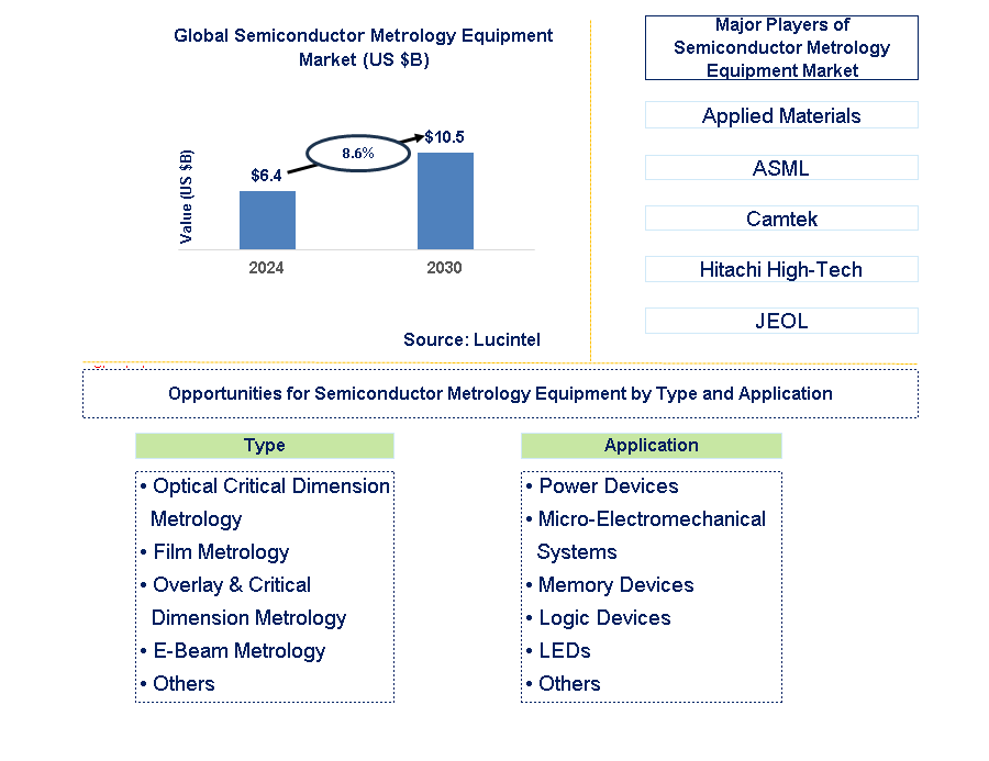
Key data points: The market size in 2030 = $10.5 billion, growth forecast = 8.6% annually for the next 6 years. Scroll below to get more insights. This market report covers trends, opportunities, and forecasts in the global semiconductor metrology equipment market to 2030 by type (optical critical dimension metrology, film metrology, overlay & critical dimension metrology, e-beam metrology, and others), application (power devices, micro-electromechanical system, memory devices, logic devices, LEDs, and others), and region (North America, Europe, Asia Pacific, and the Rest of the World)
We'll send your sample report shortly.
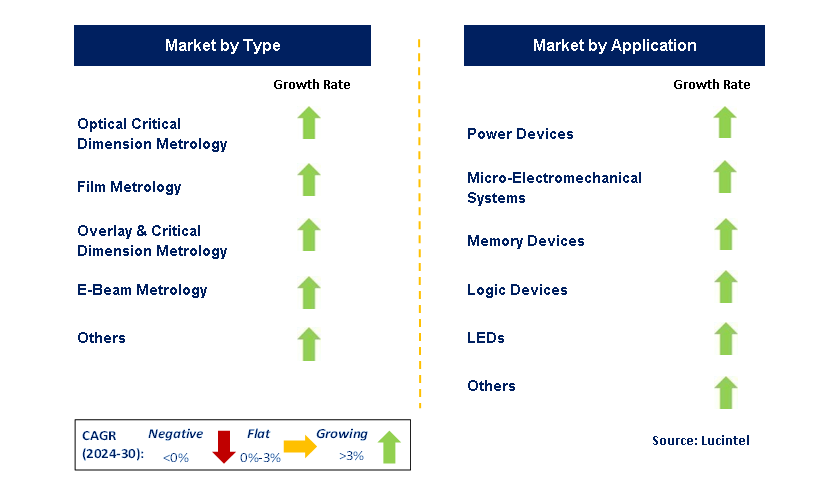
• Lucintel forecasts that, within the type category, e-beam metrology will remain the largest segment over the forecast period as it helps in ensuring the quality, reliability, and performance of semiconductor devices.
• Within the application category, logic device is expected to witness the highest growth due to growing demand of high performance and quality in logic devices.
• In terms of regions, APAC will remain the largest region over the forecast period due to increased research and development spendings and presence of major players in this region. Gain valuable insight for your business decisions with our comprehensive 150+ page report. The demand for precision in semiconductor manufacturing has led to significant advancements in semiconductor metrology equipment. These developments are driven by the increased complexity of chips, technological progress, and the expansion of the electronics industry globally. Key markets such as the United States, China, Germany, India, and Japan are making significant strides toward meeting evolving industry standards and technological demands.
• United States: In addition to AI integration, machine learning is being incorporated into semiconductor metrology equipment to enhance precision in manufacturing. U.S. companies continue to invest heavily in second-generation equipment to handle the complexity of 7nm and smaller process nodes. There is also growing pressure to develop advanced packaging technologies and 3D ICs.
• China: China is rapidly expanding its semiconductor manufacturing capacity, creating greater demand for advanced metrology equipment. The country is focusing on developing domestic metrology solutions to reduce dependency on foreign suppliers. Policies supporting semiconductor production have incentivized the creation of more local fabs and further metrology advancements.
• Germany: Germany has established itself as a leader in the high-precision measurement sector, with semiconductor metrology equipment being an essential part of this sector. High-tech companies are leveraging advanced metrology tools to enhance manufacturing processes for semiconductors. Investments are being made into expanding their presence in the semiconductor industry to maintain global competitiveness.
• India: India is growing in terms of semiconductor manufacturing with government policies supporting the development of fabs and manufacturing plants. As India invests in enhancing its semiconductor production capacity, demand for state-of-the-art metrology equipment will follow suit to ensure the highest quality standards.
• Japan: Japan is another leading market for semiconductor metrology equipment, with firms specializing in equipment for next-generation semiconductor processes. Investments in R&D and collaborations with international players are further enhancing their capabilities to meet the demands of high-performance chips. By capitalizing on these trends and market conditions, the semiconductor metrology equipment market can continue to expand and support the rapid technological advancements needed by the semiconductor industry. Gain valuable insights for your business decisions with our 150+ page report.
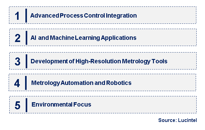
• Advanced Process Control Integration: The application of advanced process control (APC) systems integrated with metrology equipment is becoming more widespread. This enhances the current capabilities of real-time manufacturing process monitoring and correction, increasing yield and reducing defects. The data provided by metrology tools in an APC system is applied to optimize production, thereby improving efficiency and consistency in semiconductor manufacturing.
• AI and Machine Learning Applications: The use of artificial intelligence (AI) and machine learning in semiconductor metrology is increasing. AI algorithms analyze large amounts of data provided by metrology tools to identify patterns, predict potential issues, and adjust process parameters. This integration improves accuracy and reduces human error, thus contributing to greater efficiency in semiconductor production.
• Development of High-Resolution Metrology Tools: Smaller process nodes are driving the demand for high-resolution metrology tools. These tools enable higher-resolution measurements of semiconductor features in advanced manufacturing processes. High-resolution capabilities support the production of smaller and more complex semiconductor devices.
• Metrology Automation and Robotics: Metrology equipment increasingly relies on automation and robotics to reduce manual involvement in measurement processes. Automated systems offer improved throughput and consistency by minimizing human error. These systems also provide continuous high-speed measurements, which are essential in large-scale semiconductor manufacturing.
• Environmental Focus: There is growing attention on providing environmentally sustainable metrology solutions. Companies are working to minimize the environmental impact of metrology equipment by designing energy-efficient systems, reducing waste, and using recyclable materials. This trend aligns with the broader movement toward more sustainable manufacturing practices in the semiconductor industry. AI, automation, high-resolution tools, and sustainability are some of the emerging trends that are reshaping the semiconductor metrology equipment market. In light of these trends, the drive for higher precision, efficiency, and reduced environmental impact positions the industry well to meet the demands of next-generation semiconductor technologies and remain competitive in a rapidly changing market.
• High-Resolution Metrology Tools with Increased Capability: Recent advancements in high-resolution metrology tools have enabled much more precise measurement of semiconductor features. These tools are crucial for supporting the manufacture of smaller and more intricate devices at 5nm and 3nm process nodes. They help ensure better yield and performance in semiconductor manufacturing.
• Integration of AI and Machine Learning: AI and machine learning are now incorporated into metrology equipment, transforming the industry. These technologies enable advanced data analytics, predictive maintenance, and process optimization, which improve accuracy and efficiency in semiconductor manufacturing. AI-driven insights are used to address complex challenges and enhance overall production quality.
• More Automation and Robotics: Metrology systems are increasingly integrated with automation and robotics to facilitate high-speed, consistent measurements. Automated systems reduce human intervention, minimizing errors while boosting throughput. This makes automation essential for high-volume semiconductor manufacturing processes, ensuring efficiency and scalability.
• Development of Advanced Process Control Systems: Advanced process control systems integrated with metrology tools provide real-time monitoring and correction of manufacturing processes. These systems optimize production parameters, improving yield and reducing defects, ensuring quality and performance consistency in semiconductor devices.
• Environmental Sustainability: There is growing interest in environmentally friendly metrology solutions. Companies are investing in energy-efficient designs, minimizing waste, and using recyclable materials in their equipment. This focus on sustainability aligns with broader industry goals to reduce environmental impact and promote responsible manufacturing. Recent developments in the semiconductor metrology equipment market focus on advanced technology and process optimization. The integration of AI, automation, APC systems, and sustainability efforts has driven improvements in precision, efficiency, and environmental impact throughout the forecast period, ensuring further market growth and development.
• Advanced Packaging Technologies: Emerging advanced packaging technologies, such as 3D ICs and heterogeneous integration, offer significant growth potential for semiconductor metrology. These technologies require highly accurate metrology solutions to ensure proper alignment and reliable performance. As a result, there will be increased demand for advanced packaging metrology tools to support the fabrication of sophisticated semiconductor devices.
• Automotive Electronics: The growing use of ADAS and electric vehicles (EVs) presents substantial opportunities for metrology equipment in the automotive sector. Automotive electronics require highly accurate and reliable testing, necessitating sophisticated metrology solutions to ensure the quality and safety of components. This will lead to increased demand for metrology tools tailored to the automotive industry.
• IoT Devices: The proliferation of IoT devices creates growth opportunities for metrology equipment. These systems require compact, efficient, and reliable semiconductor components. The miniaturization and performance enhancement of semiconductor components will drive the need for high-precision metrology tools to support these advancements. Solution developers specializing in metrology for IoT devices will benefit from this growing market.
• Semiconductor Manufacturing Process Nodes: Advances in semiconductor manufacturing to smaller nodes, such as 5nm and 3nm, have increased the demand for advanced metrology equipment. Smaller process nodes require even more accurate measurements to ensure performance and yield. The development of metrology tools capable of handling these advanced nodes presents a significant growth opportunity in the market.
• Emerging Markets and Regional Expansion: The growth of semiconductor manufacturing in emerging markets, such as India and Southeast Asia, presents additional opportunities for metrology equipment. As these regions expand their semiconductor industries, demand for metrology solutions will increase. Companies that position themselves early in these growing markets with specialized solutions will be well positioned for success. These strategic growth opportunities in the semiconductor metrology equipment market are related to the expansion of advanced packaging technologies, automotive electronics, IoT devices, smaller process nodes, and regional expansion. Capitalizing on these opportunities will help companies achieve growth while addressing the needs of a rapidly evolving semiconductor market.
• Technological Developments: Advancements in technology are among the primary drivers of the semiconductor metrology equipment market. Factors contributing to better resolution imaging, integration with AI, and automation for measurement precision are evident. Technological advancements encourage the miniaturization and increased complexity of semiconductor devices, driving demand for state-of-the-art metrology solutions.
• High-Performance Semiconductors - Growing Demand: The increasing demand for high-performance semiconductor devices across industries such as consumer electronics, automotive, and IoT drives the need for metrology equipment. As performance requirements rise, there is a greater need for precision and reliability in measurement instrumentation to ensure the functionality and quality of these devices.
• Capacity Expansion in Semiconductor Manufacturing: The growth of semiconductor manufacturing facilities worldwide stimulates the demand for metrology equipment. Advanced metrology tools installed in new fabs and production lines further promote market growth by ensuring accurate measurements and quality control throughout the manufacturing process. Challenges in the semiconductor metrology equipment market include:
• High Development and Production Costs: High-end metrology equipment requires substantial investments in development and production. The high cost of R&D and the complexity of manufacturing create barriers to entry for new players and reduce profitability for incumbents. Managing these costs while maintaining competitive pricing is a significant challenge.
• Complexity and Integration of Technology: The increasing complexity of semiconductor manufacturing processes and device structures presents a challenge for metrology equipment. As the industry pushes boundaries, the development of features and the compatibility of evolving technologies are ongoing tasks that can become burdensome for manufacturers.
• Regulatory and Compliance Requirements: Some regions impose stringent regulatory and compliance requirements on manufacturers of metrology equipment. This increases the complexity of product development and market entry due to the need to comply with environmental regulations, quality standards, and industry-specific requirements, influencing the overall market dynamics. The driving factors for the semiconductor metrology equipment market include technological advances, the growing demand for high-performance semiconductors, expanding manufacturing capacity, advanced packaging, and the complexity of semiconductor devices. Challenges include high development costs, technological complexity, and regulatory issues. Balancing these drivers and challenges will determine success in such a competitive market.
• Applied Materials
• ASML
• Camtek
• Hitachi High-Tech
• JEOL
• KLA
• Nova
• Onto Innovation
• Thermo Fisher Scientific
• Unity Semiconductor
• Optical Critical Dimension Metrology
• Film Metrology
• Overlay & Critical Dimension Metrology
• E-Beam Metrology
• Others
• Power Devices
• Micro-Electromechanical Systems
• Memory Devices
• Logic Devices
• LEDs
• Others
• North America
• Europe
• Asia Pacific
• The Rest of the World
• United States: In addition to AI integration, machine learning is being incorporated into semiconductor metrology equipment to enhance precision in manufacturing. U.S. companies continue to invest heavily in second-generation equipment to handle the complexity of 7nm and smaller process nodes. There is also growing pressure to develop advanced packaging technologies and 3D ICs.
• China: China is rapidly expanding its semiconductor manufacturing capacity, creating greater demand for advanced metrology equipment. The country is focusing on developing domestic metrology solutions to reduce dependency on foreign suppliers. Policies supporting semiconductor production have incentivized the creation of more local fabs and further metrology advancements.
• Germany: Germany has established itself as a leader in the high-precision measurement sector, with semiconductor metrology equipment being an essential part of this sector. High-tech companies are leveraging advanced metrology tools to enhance manufacturing processes for semiconductors. Investments are being made into expanding their presence in the semiconductor industry to maintain global competitiveness.
• India: India is growing in terms of semiconductor manufacturing with government policies supporting the development of fabs and manufacturing plants. As India invests in enhancing its semiconductor production capacity, demand for state-of-the-art metrology equipment will follow suit to ensure the highest quality standards.
• Japan: Japan is another leading market for semiconductor metrology equipment, with firms specializing in equipment for next-generation semiconductor processes. Investments in R&D and collaborations with international players are further enhancing their capabilities to meet the demands of high-performance chips. By capitalizing on these trends and market conditions, the semiconductor metrology equipment market can continue to expand and support the rapid technological advancements needed by the semiconductor industry.
• Applied Materials
• ASML
• Camtek
• Hitachi High-Tech
• JEOL
• KLA
• Nova
• Onto Innovation
• Thermo Fisher Scientific
• Unity Semiconductor Q6. Which semiconductor metrology equipment market segment will be the largest in future? Answer: Lucintel forecasts that e-beam metrology will remain the largest segment over the forecast period as it helps in ensuring the quality, reliability, and performance of semiconductor devices. Q7. In semiconductor metrology equipment market, which region is expected to be the largest in next 5 years? Answer: APAC will remain the largest region over the forecast period due to increased research and development spendings and presence of major players in this region. Q.8 Do we receive customization in this report? Answer: Yes, Lucintel provides 10% customization without any additional cost.


Choose a license that fits your team. Instant PDF delivery.
Prices exclude taxes. Instant delivery. Custom licensing available on request.
Market Report · July 24, 2026
Market Report · July 20, 2026
Market Report · July 20, 2026
Trusted partner for strategic intelligence and business growth


Receive a complimentary market analysis tailored to your industry. Our analysts will identify key growth opportunities and competitive dynamics specific to your business.

Market size, growth rate, and key trend analysis for your specific sector.

Top competitor positioning and market share analysis.

Strategic recommendations backed by data-driven insights.
Get curated market intelligence and competitive moves straight to your inbox.
By subscribing, you agree to receive our monthly insights. Unsubscribe anytime.
Receive a complimentary market analysis tailored to your industry. Our analysts will identify key growth opportunities and competitive dynamics specific to your business.
Market size, growth rate, and key trend analysis for your specific sector.
Top competitor positioning and market share analysis.
Strategic recommendations backed by data-driven insights.
Get curated market intelligence, emerging trends, and competitive moves straight to your inbox each month.
By subscribing, you agree to receive our monthly insights. Unsubscribe anytime.
We'll send your sample report shortly.