
Market Report · July 22, 2026

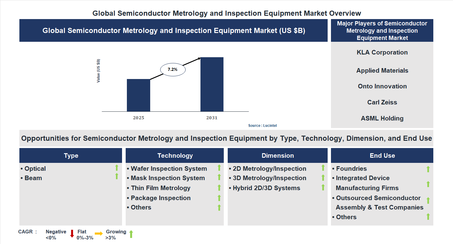
Key data points: The growth forecast = 7.2% annually for the next 7 years. Scroll below to get more insights. This market report covers trends, opportunities and forecasts in semiconductor metrology and inspection equipment market to 2031 by type (optical and beam), technology (wafer inspection system, mask inspection system, thin film metrology, package inspection, and others), dimension (2d metrology/inspection, 3d metrology/inspection, and hybrid 2d/3d systems), end use (foundries, integrated device manufacturing firms, outsourced semiconductor assembly & test companies, and others), and region (North America, Europe, Asia Pacific, and the Rest of the World)
We'll send your sample report shortly.
• Lucintel forecasts that, within the type category, optical is expected to witness higher growth over the forecast period.
• Within the end use category, foundry is expected to witness the highest growth.
• In terms of region, APAC is expected to witness the highest growth over the forecast period. Gain valuable insights for your business decisions with our comprehensive 150+ page report. Sample figures with some insights are shown below.
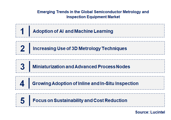
• Adoption of AI and Machine Learning: The integration of artificial intelligence and machine learning algorithms into metrology and inspection tools is transforming the industry. These technologies enable real-time data analysis, defect detection, and process optimization, significantly reducing inspection times and improving accuracy. Companies like ASML and kLA are leveraging AI to enhance their equipment capabilities, leading to smarter, more autonomous systems. This trend improves yield rates, reduces costs, and accelerates time-to-market for semiconductor products, making AI-driven solutions a critical component of future metrology and inspection strategies.
• Increasing Use of 3D Metrology Techniques: The shift from 2D to 3D metrology methods is driven by the need for more comprehensive inspection of complex, multi-layered semiconductor devices. 3D techniques such as atomic force microscopy (AFM) and X-ray tomography provide detailed insights into device structures, ensuring higher precision and defect detection. Companies like hitachi and zeiss are expanding their 3D metrology offerings to meet industry demands. This trend enhances the ability to identify manufacturing flaws early, reducing waste and improving overall device performance, which is vital for advanced semiconductor nodes.
• Miniaturization and Advanced Process Nodes: As the industry moves towards smaller process nodes (7nm, 5nm, and below), the demand for ultra-precise metrology and inspection equipment increases. These advanced nodes require tools capable of measuring features at the atomic level, pushing companies to innovate rapidly. firms like nanometrics and kLA are developing high-resolution systems to meet these needs. This trend ensures that manufacturers can maintain tight process control, improve yields, and stay competitive in a market where device miniaturization is paramount.
• Growing Adoption of Inline and In-Situ Inspection: The trend toward inline and in-situ inspection solutions is driven by the need for real-time quality control during manufacturing. These systems enable continuous monitoring without halting production, reducing downtime and increasing throughput. Companies such as asml and hitachi are investing in integrated inspection tools that can be embedded within fabrication lines. This approach enhances process control, minimizes defects, and accelerates troubleshooting, ultimately leading to higher yields and more efficient production workflows.
• Focus on Sustainability and Cost Reduction: Environmental concerns and cost pressures are prompting companies to develop more energy-efficient and cost-effective metrology solutions. Innovations include low-power systems, reduced material usage, and modular designs that lower overall costs. Firms like zeiss and nanometrics are emphasizing sustainable practices in their product development. This trend not only reduces the environmental footprint but also helps manufacturers lower operational costs, making advanced metrology more accessible and aligning with global sustainability goals. In summary, these emerging trends are fundamentally reshaping the semiconductor metrology and inspection equipment market by enhancing precision, efficiency, and sustainability. They enable manufacturers to keep pace with technological advancements, meet stringent quality standards, and reduce costs, thereby driving innovation and competitiveness in the semiconductor industry.
• Technological Advancements in AI-Driven Inspection: The integration of artificial intelligence into inspection tools has enhanced defect detection accuracy and speed. Companies like asml and kLA are developing AI-powered systems that enable real-time analysis, reducing false positives and increasing throughput. This innovation improves yield rates and reduces manufacturing costs, making it a critical advancement for high-volume production.
• Expansion of 3D Metrology Techniques: The adoption of 3D measurement technologies, such as X-ray and optical coherence tomography, has increased. These techniques allow for detailed analysis of complex 3D structures in semiconductors, improving defect identification and process control. Companies like nanometrics and zeiss are leading this development, which enhances precision and reduces time-to-market for advanced chips.
• Increased Adoption of Inline Inspection Systems: Inline inspection solutions are becoming more prevalent, enabling real-time monitoring during manufacturing. This reduces downtime and enhances process control. firms like kLA and asml are expanding their inline inspection offerings, which significantly improve yield and reduce scrap rates, thus boosting overall efficiency.
• Focus on EUV (Extreme Ultraviolet) Metrology: As EUV lithography becomes mainstream, specialized metrology tools for EUV are being developed. These tools ensure the accuracy of EUV patterning, critical for next-generation nodes. Companies such as asml and veeco are investing in EUV-specific metrology, which is vital for maintaining precision at smaller nodes and supporting Moores Law.
• Rising Investment in R&D and Strategic Collaborations: Major players are increasing R&D budgets and forming strategic alliances to develop next-generation inspection and metrology solutions. Collaborations between firms like asml, kLA, and imec are fostering innovation, accelerating product development, and expanding market reach. This trend ensures continuous technological evolution and market competitiveness. In summary, these developments are significantly transforming the semiconductor metrology and inspection equipment market by enhancing precision, efficiency, and technological capabilities. The integration of AI, advanced 3D techniques, inline systems, EUV-specific tools, and increased R&D investments are driving innovation, reducing costs, and enabling the industry to meet the demands of next-generation semiconductor manufacturing. These changes are positioning the market for sustained growth and increased competitiveness in the evolving semiconductor landscape.
• Advanced Process Control: Improving yield and reducing defects through real-time monitoring and adjustments, leading to higher manufacturing efficiency and lower costs.
• 3D Metrology Solutions: Enabling precise measurement of complex 3D structures in advanced chips, which enhances device performance and reliability.
• AI-Driven Inspection: Utilizing artificial intelligence for faster defect detection and analysis, increasing throughput and reducing human error.
• Nano-Scale Inspection: Addressing the challenges of inspecting at the atomic level, crucial for next-generation semiconductor devices.
• Packaging and Assembly Inspection: Ensuring the integrity of semiconductor packaging, which is vital for device protection and performance. These growth opportunities are significantly impacting the market by driving innovation, improving manufacturing precision, and enabling the production of more complex and reliable semiconductor devices. Companies like KLA, ASML, and lam research are at the forefront, leveraging these opportunities to expand their market share and meet the evolving demands of the semiconductor industry.
• Technological Innovation: The continuous evolution of semiconductor manufacturing processes necessitates advanced metrology and inspection tools. As device architectures become more complex, with smaller nodes and 3D structures, the demand for high-precision measurement equipment increases. Innovations such as AI-driven inspection systems and automation enhance accuracy and efficiency, reducing defect rates and improving yield. These technological advancements enable manufacturers to meet stringent quality standards, accelerate time-to-market, and maintain competitive advantage, thereby fueling market growth.
• Growing Semiconductor Demand: The surge in demand for semiconductors across various sectors like consumer electronics, automotive, and data centers drives the need for sophisticated metrology and inspection solutions. The proliferation of IoT, 5G, and AI applications has expanded the semiconductor market, prompting manufacturers to invest heavily in quality control tools. This increased production volume and complexity necessitate reliable inspection equipment to ensure product integrity, ultimately propelling market expansion.
• Industry Consolidation and Strategic Partnerships: Major players in the semiconductor industry are forming alliances and consolidating to enhance technological capabilities and market reach. Collaborations between equipment manufacturers and semiconductor fabs facilitate the development of tailored solutions, fostering innovation. These strategic partnerships enable faster deployment of new technologies, improve supply chain resilience, and expand market share, thus positively impacting the growth trajectory of the metrology and inspection equipment market.
• Regulatory and Quality Standards: Stringent regulatory requirements related to environmental safety, product quality, and safety standards influence the adoption of advanced inspection tools. Compliance with international standards such as ISO and SEMI ensures product reliability and reduces liability risks. These regulations compel manufacturers to invest in sophisticated metrology solutions that can meet or exceed compliance benchmarks, thereby driving market demand and encouraging technological upgrades. The challenges facing this semiconductor metrology and inspection equipment market include:
• High Capital and Operational Costs: The deployment of advanced metrology and inspection equipment involves significant capital investment and operational expenses. The high costs of equipment, maintenance, and skilled personnel can be prohibitive, especially for smaller players. This financial barrier limits market entry and expansion, constraining overall growth. Additionally, rapid technological obsolescence necessitates frequent upgrades, further increasing costs and impacting profitability.
• Rapid Technological Changes: The fast-paced evolution of semiconductor manufacturing technologies creates a challenge for equipment providers to keep pace. Developing tools that can adapt to new process nodes and architectures requires substantial R&D investment and innovation. Failure to keep up can result in outdated solutions, reduced competitiveness, and loss of market share. This constant need for technological adaptation complicates product development cycles and increases risk for companies.
• Supply Chain Disruptions: Global supply chain issues, including shortages of critical components and logistical delays, significantly impact the production and delivery of metrology and inspection equipment. These disruptions can lead to project delays, increased costs, and reduced customer satisfaction. The dependency on a complex supply network makes the market vulnerable to geopolitical tensions, pandemics, and trade restrictions, which can hinder growth and innovation efforts. In summary, the semiconductor metrology and inspection equipment market is shaped by rapid technological advancements, increasing demand driven by semiconductor industry growth, strategic industry collaborations, and regulatory compliance requirements. However, high costs, rapid technological changes, and supply chain disruptions pose significant challenges. These factors collectively influence the markets growth potential, requiring stakeholders to innovate continuously, optimize costs, and navigate geopolitical and regulatory landscapes effectively. The overall impact is a dynamic, competitive environment that demands agility and strategic foresight to capitalize on emerging opportunities.
• KLA Corporation
• Applied Materials
• Onto Innovation
• Carl Zeiss
• ASML Holding
• Camtek
• Hitachi High-Tech Corporation
• Lasertec Corporation
• Nova
• SCREEN Semiconductor Solutions
• Optical
• Beam
• Wafer Inspection System
• Mask Inspection System
• Thin Film Metrology
• Package Inspection
• Others
• 2D Metrology/Inspection
• 3D Metrology/Inspection
• Hybrid 2D/3D Systems
• Foundries
• Integrated Device Manufacturing Firms
• Outsourced Semiconductor Assembly & Test Companies
• Others
• North America
• Europe
• Asia Pacific
• The Rest of the World
• United States, companies like kla-tencor and nanometrics are leading the market with innovations in AI-powered inspection systems, expanding their R&D efforts, and forming strategic alliances to enhance product offerings. The US government is also investing in advanced research initiatives to support domestic semiconductor manufacturing.
• China is rapidly advancing with companies such as shanghai microelectronics and kingsemi, focusing on developing indigenous metrology solutions. The government’s policies aim to reduce reliance on imports, and there is significant investment in local R&D and manufacturing infrastructure to boost self-sufficiency.
• Germany’s key players, including carl zeiss and essilor, are emphasizing high-precision optical inspection tools and integrating automation technologies. The country is also focusing on sustainable manufacturing practices and collaborating with European research institutions to innovate in metrology techniques.
• India’s market is witnessing growth through companies like sumeet and sgs, which are expanding their inspection capabilities and adopting new technologies such as AI and machine learning. The government’s initiatives to promote semiconductor manufacturing are encouraging local industry development and attracting foreign investments.
• Japan remains a significant player with companies such as tokyo electron and hitachi, focusing on advanced inspection systems and miniaturization technologies. The country is investing in next-generation metrology solutions to support its semiconductor ecosystem and maintain technological leadership.
• KLA Corporation
• Applied Materials
• Onto Innovation
• Carl Zeiss
• ASML Holding
• Camtek
• Hitachi High-Tech Corporation
• Lasertec Corporation
• Nova
• SCREEN Semiconductor Solutions Q5. Which semiconductor metrology and inspection equipment market segment will be the largest in future? Answer: Lucintel forecasts that, within the type category, optical is expected to witness higher growth over the forecast period. Q6. In semiconductor metrology and inspection equipment market, which region is expected to be the largest in next 5 years? Answer: In terms of region, APAC is expected to witness the highest growth over the forecast period. Q7. Do we receive customization in this report? Answer: Yes, Lucintel provides 10% customization without any additional cost.


Choose a license that fits your team. Instant PDF delivery.
Prices exclude taxes. Instant delivery. Custom licensing available on request.
Market Report · July 22, 2026
Market Report · July 17, 2026
Market Report · July 17, 2026
Trusted partner for strategic intelligence and business growth


Receive a complimentary market analysis tailored to your industry. Our analysts will identify key growth opportunities and competitive dynamics specific to your business.

Market size, growth rate, and key trend analysis for your specific sector.

Top competitor positioning and market share analysis.

Strategic recommendations backed by data-driven insights.
Get curated market intelligence and competitive moves straight to your inbox.
By subscribing, you agree to receive our monthly insights. Unsubscribe anytime.
Receive a complimentary market analysis tailored to your industry. Our analysts will identify key growth opportunities and competitive dynamics specific to your business.
Market size, growth rate, and key trend analysis for your specific sector.
Top competitor positioning and market share analysis.
Strategic recommendations backed by data-driven insights.
Get curated market intelligence, emerging trends, and competitive moves straight to your inbox each month.
By subscribing, you agree to receive our monthly insights. Unsubscribe anytime.
We'll send your sample report shortly.