
Market Report · July 24, 2026

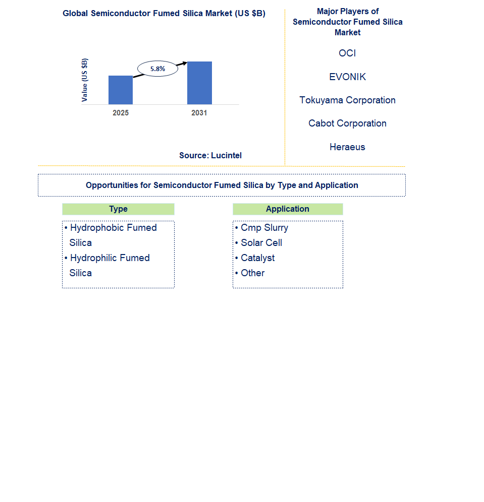
Key data points: The growth forecast = 0.058 annually for the next 7 years. Scroll below to get more insights. This market report covers Trends, opportunities and forecasts in semiconductor fumed silica market to 2031 by type (hydrophobic fumed silica and hydrophilic fumed silica), application (cmp slurry, solar cell, catalyst, and other), and region (North America, Europe, Asia Pacific, and the Rest of the World)
We'll send your sample report shortly.
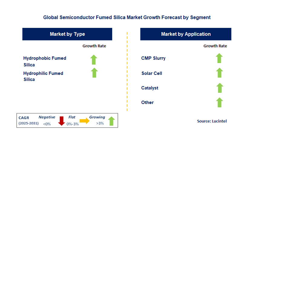
• Lucintel forecasts that, within the type category, hydrophobic fumed silica, and hydrophilic fumed silica is expected to witness higher growth over the forecast period due to increasing demand for moisture-resistant applications.
• Within the application category, cmp slurry, solar cell, and catalyst is expected to witness the highest growth due to rising demand in semiconductor wafer polishing processes.
• In terms of region, APAC is expected to witness the highest growth over the forecast period due to leading semiconductor manufacturing and technological advancements.
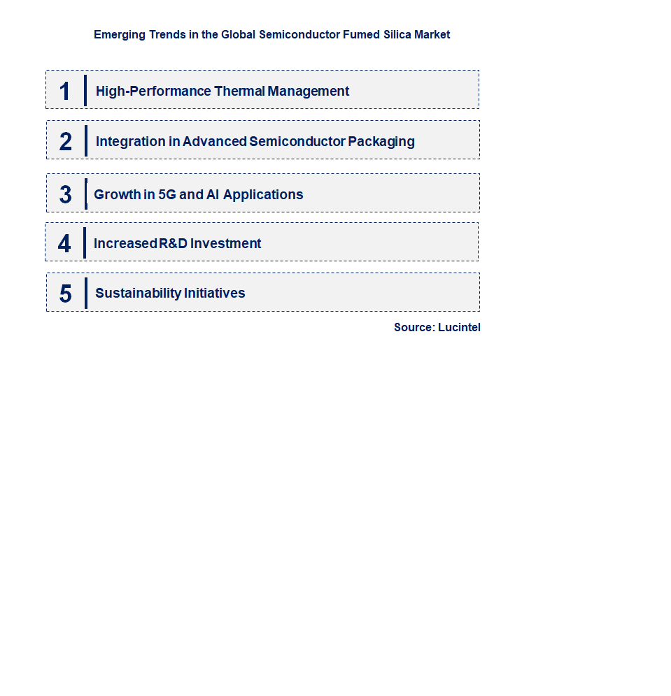
• High-Performance Thermal Management: Fumed silica is now being increasingly adopted by semiconductor companies as the demand for efficient heat dissipation is on the rise. It provides excellent insulation, making it the best material for high-performance semiconductor devices that need advanced thermal management solutions.
• Integration in Advanced Semiconductor Packaging: Fumed silica is used in developing advanced packaging materials. It increases the performance and durability of semiconductor components, particularly in automotive, consumer electronics, and telecommunications.
• Growth in 5G and AI Applications: Fumed silica is being adopted in the manufacturing of AI and 5G chip technologies. Its role in improving the reliability and longevity of semiconductor devices is critical for enabling the performance required by these cutting-edge technologies.
• Increased R&D Investment: Companies are investing heavily in R&D to explore new ways of utilizing fumed silica in semiconductor applications. These innovations are focused on improving the properties of fumed silica, such as its compatibility with high-frequency semiconductor applications and enhancing its insulating qualities.
• Sustainability Initiatives: As environmental concerns keep rising, the semiconductor industry has been focusing more on eco-friendly production methods. Sustainable fumed silica production techniques and recycling methodologies are being considered to reduce material environmental impact without compromising market demands.
• The semiconductor fumed silica market is rapidly evolving as breakthroughs in manufacturing and material science fuel its growth. The significant steps are related to progress in the production process, new applications, and advancements in semiconductor technology. This places fumed silica in a crucial position for next-generation semiconductor applications.
• Improvements in Production Methods: Manufacturers are upgrading production processes to make fumed silica more uniform and pure. These improvements will be necessary for the increasing demands of high-performance materials in semiconductor manufacturing.
• Integration in Next-Generation Semiconductor Devices: Fumed silica is finding applications in state-of-the-art semiconductor devices such as AI, 5G, and high-frequency chips. Its properties will be critical for enhancing the efficiency and performance of these devices.
• Development of Custom Formulations: The manufactures are coming up with specialized fumed silica formulations to meet various semiconductor-specific requirements. These custom formulations are mainly designed for improved chip packaging, thermal stability, and electrical insulation.
• Focus on Sustainable Manufacturing: With environmental factors on the rise, the industry is pushing for sustainability in manufacturing processes while producing fumed silica. Energy consumption, waste, and environmental impact are reduced at the same time, but the qualities of products remain high.
• Collaborations for Technology Advancements: Fumed silica companies and materials suppliers are teaming up for strategic partnerships for the acceleration of technological innovations within fumed silica applications. It is through such collaborations that they drive new product developments and also improve material performance for semiconductor devices.
The above mentioned are the primary developments that make the semiconductor fumed silica market grow. The production innovations, new applications, and sustainable practices strengthen the fumed silica in advanced semiconductor manufacturing.• Thermal Management Solutions: The demand for efficient heat dissipation is rising, and thus, the fumed silica used in semiconductor thermal management solutions opens up a massive growth opportunity. It is a critical component to ensure the lifespan and reliability of advanced chips.
• Semiconductor Packaging Applications: The application of fumed silica in semiconductor packaging is expanding, particularly in automotive and consumer electronics. This application is crucial for the enhancement of the durability and performance of semiconductor devices.
• 5G and AI Semiconductor Applications: The necessity for high-performance semiconductors has been driven by the rising trends of 5G and AI technologies. Fumed silica is critical in enhancing the performance and efficiency of the chips used in these applications.
• Power Electronics Manufacturing: The power semiconductors are needed in the industries of automotive and renewable energy. Due to insulating properties, the fumed silica is considered a material in manufacturing power electronics, and because of this, growth prospects exist in the sector.
• Advances in Nanoelectronics: As semiconductor technology continues toward a smaller and more potent tool, fumed silica will take the most important place in the advancement of nanoelectronics across higher performance and efficiency.
These strategic growth opportunities are shaping the future of the semiconductor fumed silica market. As demand for high-performance materials continues to increase, fumed silica will increasingly play an important role in advancing semiconductor technology across various applications.• OCI
• EVONIK
• Tokuyama Corporation
• Cabot Corporation
• Heraeus
• Hydrophobic Fumed Silica
• Hydrophilic Fumed Silica
• Cmp Slurry
• Solar Cell
• Catalyst
• Other
• North America
• Europe
• Asia Pacific
• The Rest of the World
• United States: The U.S. semiconductor fumed silica market is growing due to the increasing demand for advanced manufacturing processes. Major semiconductor companies are using fumed silica to enhance the performance and reliability of chips. In addition, major R&D investments are targeted at developing specialized formulations for high-precision semiconductor applications.
• China: China is accelerating its semiconductor manufacturing capabilities and using more fumed silica in the production process. As the country continues to boost its domestic supply chain for semiconductors, local producers are improving production methods for fumed silica in order to address the increasing need for advanced semiconductor materials, such as those applied in 5G and AI.
• Germany: Fumed silica is being integrated into the semiconductor industry in Germany for encapsulation and insulation in chip packaging. The automotive and industrial semiconductor applications require very high-performance and abrasion-resistant product from fumed silica. Research collaborations are designed to develop future innovations in fumed silica's role in the improvement of thermal stability in power electronics.
• India: Fumed silica is steadily gaining usage in the semiconductor market of India. Its application has been focused on enhancing chip production and performance. The government's support for indigenous semiconductor manufacturing has been encouraging local producers to adopt fumed silica in their supply chains. New applications of fumed silica in semiconductors are being researched through R&D activities.
• Japan: Japan continues to lead in precision manufacturing and is utilizing fumed silica to enhance the performance of semiconductor devices. The interest is in how the material will improve thermal conductivity and electrical insulation properties. Companies in Japan are also researching novel applications of fumed silica in power electronics, especially for high-frequency chips.


• OCI
• EVONIK
• Tokuyama Corporation
• Cabot Corporation
• Heraeus
Q5. Which semiconductor fumed silica market segment will be the largest in future?

Choose a license that fits your team. Instant PDF delivery.
Prices exclude taxes. Instant delivery. Custom licensing available on request.
Market Report · July 24, 2026
Market Report · July 20, 2026
Market Report · July 20, 2026
Trusted partner for strategic intelligence and business growth


Receive a complimentary market analysis tailored to your industry. Our analysts will identify key growth opportunities and competitive dynamics specific to your business.

Market size, growth rate, and key trend analysis for your specific sector.

Top competitor positioning and market share analysis.

Strategic recommendations backed by data-driven insights.
Get curated market intelligence and competitive moves straight to your inbox.
By subscribing, you agree to receive our monthly insights. Unsubscribe anytime.
Receive a complimentary market analysis tailored to your industry. Our analysts will identify key growth opportunities and competitive dynamics specific to your business.
Market size, growth rate, and key trend analysis for your specific sector.
Top competitor positioning and market share analysis.
Strategic recommendations backed by data-driven insights.
Get curated market intelligence, emerging trends, and competitive moves straight to your inbox each month.
By subscribing, you agree to receive our monthly insights. Unsubscribe anytime.
We'll send your sample report shortly.