
Market Report · July 24, 2026

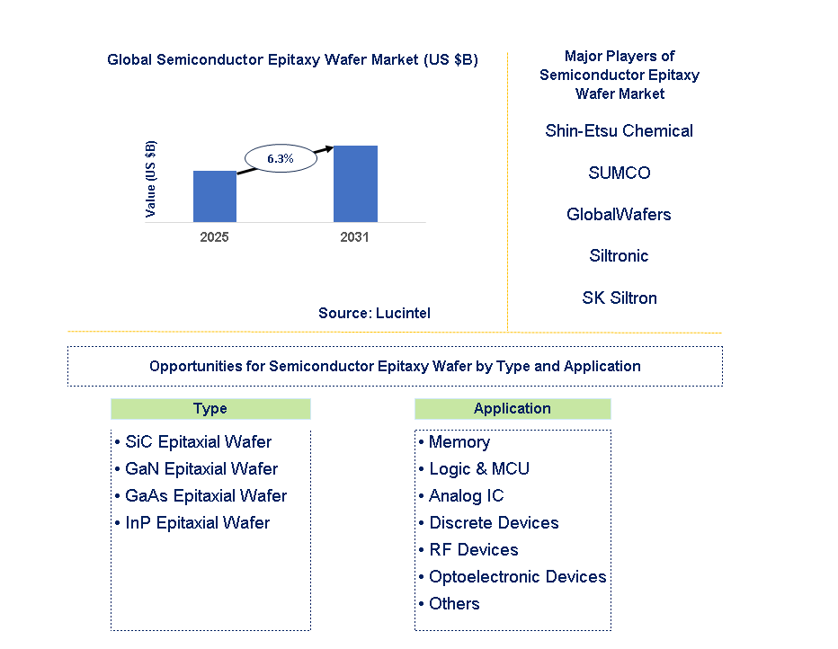
Key data points: The growth forecast = 6.3% annually for the next 7 years. Scroll below to get more insights. This market report covers trends, opportunities and forecasts in semiconductor epitaxy wafer market to 2031 by type (SiC epitaxial wafer, GaN epitaxial wafer, GaAs epitaxial wafer, and InP epitaxial wafer), application (memory, logic & MCU, analog IC, discrete devices, RF devices, optoelectronic devices, and others), and region (North America, Europe, Asia Pacific, and the Rest of the World)
We'll send your sample report shortly.
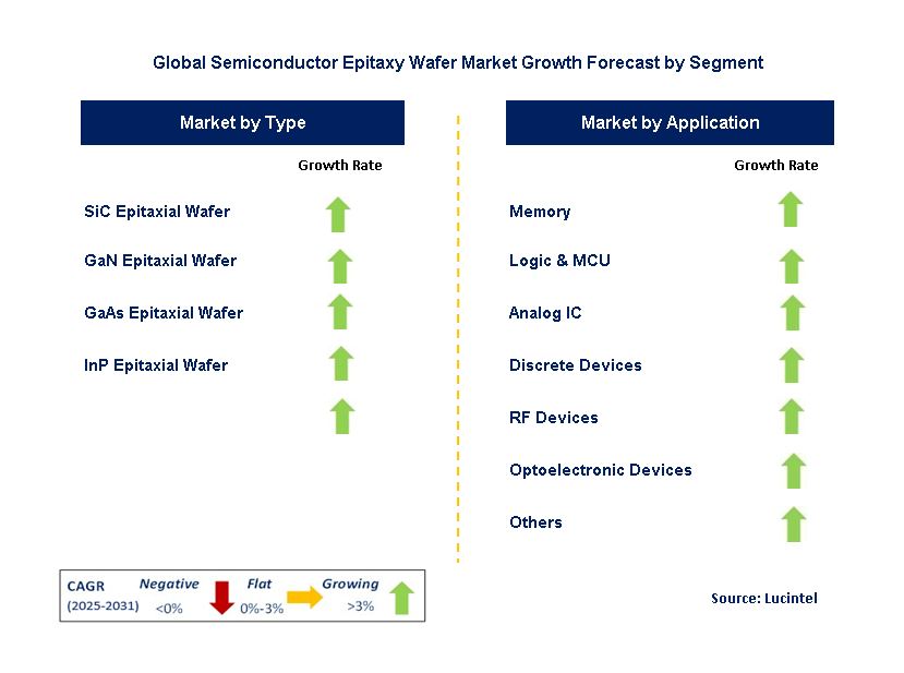
• Lucintel forecasts that, within the type category, sic epitaxial wafer is expected to witness the highest growth over the forecast period.
• Within the application category, memory is expected to witness the highest growth.
• In terms of region, APAC is expected to witness the highest growth over the forecast period. Gain valuable insights for your business decisions with our comprehensive 150+ page report. Sample figures with some insights are shown below.
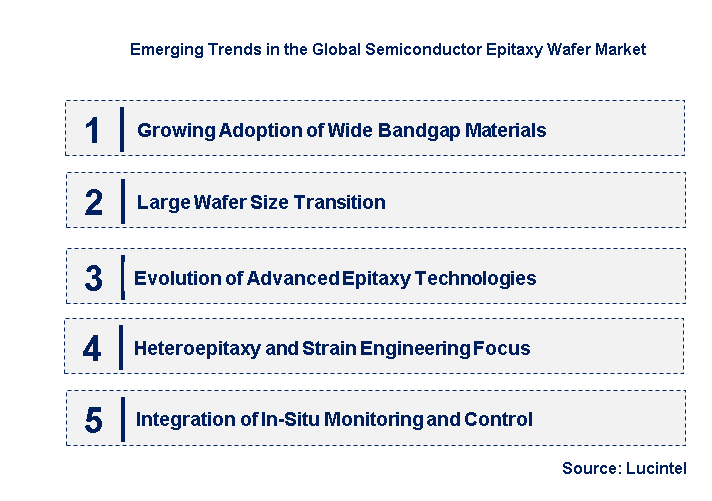
• Growing Adoption of Wide Bandgap Materials: There is a strong trend toward the increased adoption of wide bandgap (WBG) materials such as silicon carbide (SiC) and gallium nitride (GaN) for epitaxy. These materials provide better properties than silicon for high-power and high-frequency applications. The need for SiC and GaN epitaxial wafers is increasing, fueled by the expansion of electric vehicles, renewable energy systems, and sophisticated communication technologies, resulting in rigorous research and development work in this field.
• Large Wafer Size Transition: The semiconductor sector keeps forging ahead with larger wafer sizes to enhance manufacturing effectiveness and lower per-chip costs. Although silicon epitaxy has in great part shifted to 300mm wafers, momentum is gaining in increasing the wafer size for compound semiconductors such as SiC and GaN. The establishment of cost-effective and high-quality epitaxy on bigger WBG wafers is one of the prime areas to address rising volume needs.
• Evolution of Advanced Epitaxy Technologies: To obtain the highly controlled layer thickness, doping concentration, and material composition needed for advanced devices, there is ongoing evolution of advanced epitaxy technologies. They involve atomic layer epitaxy (ALE), metal-organic chemical vapor deposition (MOCVD) with enhanced reactor designs, and molecular beam epitaxy (MBE) for niche applications. These new technologies allow for the growth of ultra-thin films with outstanding uniformity and interface quality.
• Heteroepitaxy and Strain Engineering Focus: Heteroepitaxy, the epitaxial growth of a crystalline film on a substrate of dissimilar material, is increasingly relevant for combining materials with disparate properties to optimize device function. Strain engineering, the deliberate incorporation of strain in the epitaxial layer to change its electronic properties, is another dominant trend. Accurate control of the heteroepitaxial structure‘s interface and strain is important for next-generation transistors and optoelectronic devices.
• Integration of In-Situ Monitoring and Control: To enhance epitaxial layer yield and uniformity, attention is being focused more and more on integrating in-situ monitoring and control systems with epitaxy reactors. Real-time growth parameter monitoring of temperature, pressure, and gas flow enables in-process dynamic adjustment, resulting in more uniform and high-quality epitaxial wafers. Integration of in-situ monitoring and control is essential to obtain the tight tolerances needed for next-generation semiconductor manufacturing. These new trends are collectively redefining the semiconductor epitaxy wafer market by propelling innovation in materials, processes, and manufacturing methods. The growing use of wide bandgap materials, the move towards larger wafers, the creation of new epitaxy techniques, the emphasis on heteroepitaxy and strain engineering, and the use of in-situ monitoring are all going towards producing higher-performance and lower-cost epitaxial wafers for future electronic devices.
• Increased Crystal Quality and Lower Defect Density: One of the main areas of advancement is the ongoing enhancement in epitaxial layer crystal quality and defect densities being decreased. Better growth methods and reactor design optimization are resulting in fewer dislocations and other defects in epitaxial wafers, hence improving performance and yield in downstream device production. This is especially important for next-generation logic and memory devices.
• Power Semiconductors Epitaxy Advances: The power electronics market boom spurred by electric vehicles and renewable energy is propelling the development of epitaxy for wide bandgap material such as silicon carbide (SiC) and gallium nitride (GaN). Developments such as better doping control, thicker high-uniformity epitaxial layer growth, and basal plane dislocation reduction in SiC wafers result in more efficient and more dependable power devices.
• Epitaxial Structures for Next-Generation Transistors: For semiconductor logic and memory devices of the future, research is well underway to develop intricate epitaxial structures with ultra-thin layers and sharp interfaces. Methods like selective epitaxy and strained silicon-germanium layer growth are being improved for higher carrier mobility and better performance of next-generation FinFET and gate-all-around (GAA) transistors.
• Production Scaling Up of Large-Diameter Compound Semiconductor Wafers: In order to address the growing demand for compound semiconductors, attention is being focused on increasing production of higher diameter wafers (e.g., 8-inch and 6-inch for SiC) with good epitaxial quality. Defect and uniformity control challenges on larger area substrates need to be overcome in order to decrease the cost of devices based on these materials.
• Discovery of New Materials for Epitaxy: In addition to silicon, SiC, and GaN, efforts are being directed to other materials for niche epitaxial applications. These include gallium oxide (Ga₂O₃) for ultra-high power electronics and III-V compounds for high-end optoelectronics and high-frequency applications. Establishing robust and economical epitaxy processes for these new materials is an ongoing area of research. These advancements are profoundly affecting the semiconductor epitaxy wafer market by allowing higher-quality materials to be produced with better performance characteristics. The progress in epitaxy for power semiconductors and next-generation transistors, compound semiconductor wafer manufacturing scaling up, and research into new materials are all driving and diversifying the market.
• Power Electronics for Electric Vehicles (EVs): The fast-expanding electric vehicle market offers a large opportunity for high-quality silicon carbide (SiC) and gallium nitride (GaN) epitaxial wafers. They are essential for efficient power inverters and other power management components in EVs. Fabrication of large-diameter, low-defect density SiC and GaN epitaxial wafers with optimum doping profiles for EV applications is an important growth sector.
• Renewable Energy Systems: Solar and wind energy systems‘ growing adoption pushes the demand for effective power conversion equipment, which is based on SiC and GaN semiconductors. Providing high-performance epitaxial wafers for inverters and other control units in renewable energy systems is an important growth area. Cost-effectiveness and high reliability are key areas of focus for these applications.
• 5G and Advanced Communication Infrastructure: Implementation of 5G and next-generation communication networks demands devices with high-frequency and high-power, where GaN-based epitaxial wafers have better performance. GaN-on-SiC and GaN-on-Si epitaxial wafers with excellent RF values for power amplifiers and other communication devices are a bright area of growth.
• Advanced Display Technologies (MicroLEDs): High-quality epitaxial layers of III-V materials such as gallium nitride (GaN) and aluminum gallium indium phosphide (AlGaInP) are needed in Micro LED displays for efficient and effective emission of light. Providing epitaxial wafers with high thickness control and low density of defects for the production of Microbleeds for displays in wearables, smartphones, and large screens is a major growth prospect in the optoelectronics market.
• Photonics and Optical Communication: Growth in photonics is being propelled by the need for high-speed data communications and sophisticated sensing technologies. Epitaxial wafers of materials such as indium phosphide (InP) and gallium arsenide (GaAs) with structures designed for lasers, detectors, and other photonic devices that are employed in optical communication, LiDAR, and other sensing technologies represent a strategic growth opportunity. These growth opportunities strategically emphasize the promise of the semiconductor epitaxy wafer market to grow substantially by tapping into the unique material and performance needs of high-growth power electronics, communication, display technologies, and photonics applications. Firms that can deliver tailored and high-quality epitaxial solutions to these segments will be successful.
• Shin-Etsu Chemical
• SUMCO
• GlobalWafers
• Siltronic
• SK Siltron
• WAFER WORKS
• Shanghai Advanced Silicon Technology
• Nanjing Guosheng Electronics
• Hangzhou Lion Microelectronics
• National Silicon Industry Group
• Sic Epitaxial Wafer
• SiC Epitaxial Wafer
• GaN Epitaxial Wafer
• GaAs Epitaxial Wafer
• InP Epitaxial Wafer
• Memory
• Logic & MCU
• Analog IC
• Discrete Devices
• RF Devices
• Optoelectronic Devices
• Others
• North America
• Europe
• Asia Pacific
• The Rest of the World
• United States: The US is concentrating on strengthening its homegrown semiconductor manufacturing industry, such as the epitaxy wafer market. Some of the recent developments involve government schemes and funding to boost local manufacturing capability and develop innovations in high-end epitaxy methods for silicon carbide (SiC) and gallium nitride (GaN) materials, which are vital for power electronics and RF applications. Research organizations and industry participants are working together to speed up the development of next-generation epitaxial wafers.
• China: China is making rapid progress in enhancing its semiconductor manufacturing facilities throughout the entire value chain, including epitaxy wafer production. Current developments include major investments in the construction of new epitaxy wafer fabrication plants and enhancing the quality and yield of domestically produced wafers. There is a strong focus on becoming self-sufficient in core semiconductor materials such as silicon and compound semiconductors such as SiC and GaN epitaxial wafers to supply its growing electronics industry.
• Germany: Germany is at the forefront of the European semiconductor industry, with an emphasis on specialty semiconductors and automotive applications. Some new trends in the epitaxy wafer market are improved thin-film deposition methods for silicon-based epitaxy employed by automotive microcontrollers and sensors. Research and development of epitaxy for power semiconductors on SiC and GaN is increasing due to the improved energy efficiency needed in the automotive and industrial markets.
• India: The Indian semiconductor production environment is at an early but rapidly developing phase. Recent initiatives include government policies offering incentives to encourage investment in semiconductor fabrication and production of materials, including epitaxy wafers. The domestic capacity for current production is small, but there is strategic emphasis on capability development in silicon epitaxy to enable the expanded electronics market and possible future plans for semiconductor production. Partnerships with foreign technology suppliers are likely to be important.
• Japan: Japan has an established base in the semiconductor equipment and material markets. Developments in the recent epitaxy wafer market include an emphasis on high-purity silicon epitaxy for the latest logic and memory devices. Japanese companies are also aggressively involved in the growth and fabrication of compound semiconductor-based epitaxial wafers such as SiC and GaN for power electronics and RF applications, using their knowledge of precision manufacturing and materials science.

• Shin-Etsu Chemical
• SUMCO
• GlobalWafers
• Siltronic
• SK Siltron
• WAFER WORKS
• Shanghai Advanced Silicon Technology
• Nanjing Guosheng Electronics
• Hangzhou Lion Microelectronics
• National Silicon Industry Group Q5. Which semiconductor epitaxy wafer market segment will be the largest in future? Answer: Lucintel forecasts that, within the type category, sic epitaxial wafer is expected to witness the highest growth over the forecast period. Q6. In semiconductor epitaxy wafer market, which region is expected to be the largest in next 5 years? Answer: In terms of region, APAC is expected to witness the highest growth over the forecast period. Q7. Do we receive customization in this report? Answer: Yes, Lucintel provides 10% customization without any additional cost.


Choose a license that fits your team. Instant PDF delivery.
Prices exclude taxes. Instant delivery. Custom licensing available on request.
Market Report · July 24, 2026
Market Report · July 20, 2026
Market Report · July 20, 2026
Trusted partner for strategic intelligence and business growth


Receive a complimentary market analysis tailored to your industry. Our analysts will identify key growth opportunities and competitive dynamics specific to your business.

Market size, growth rate, and key trend analysis for your specific sector.

Top competitor positioning and market share analysis.

Strategic recommendations backed by data-driven insights.
Get curated market intelligence and competitive moves straight to your inbox.
By subscribing, you agree to receive our monthly insights. Unsubscribe anytime.
Receive a complimentary market analysis tailored to your industry. Our analysts will identify key growth opportunities and competitive dynamics specific to your business.
Market size, growth rate, and key trend analysis for your specific sector.
Top competitor positioning and market share analysis.
Strategic recommendations backed by data-driven insights.
Get curated market intelligence, emerging trends, and competitive moves straight to your inbox each month.
By subscribing, you agree to receive our monthly insights. Unsubscribe anytime.
We'll send your sample report shortly.