
Market Report · July 24, 2026

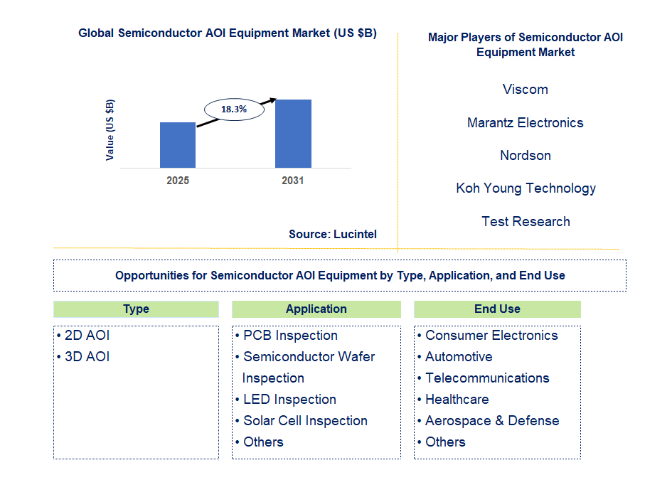
Key data points: The growth forecast = 18.3% annually for the next 7 years. Scroll below to get more insights. This market report covers trends, opportunities and forecasts in semiconductor AOI equipment market to 2031 by type (2D AOI and 3D AOI), application (PCB inspection, semiconductor wafer inspection, LED inspection, solar cell inspection, and others), end use (consumer electronics, automotive, telecommunications, healthcare, aerospace & defense, and others), and region (North America, Europe, Asia Pacific, and the Rest of the World)
We'll send your sample report shortly.
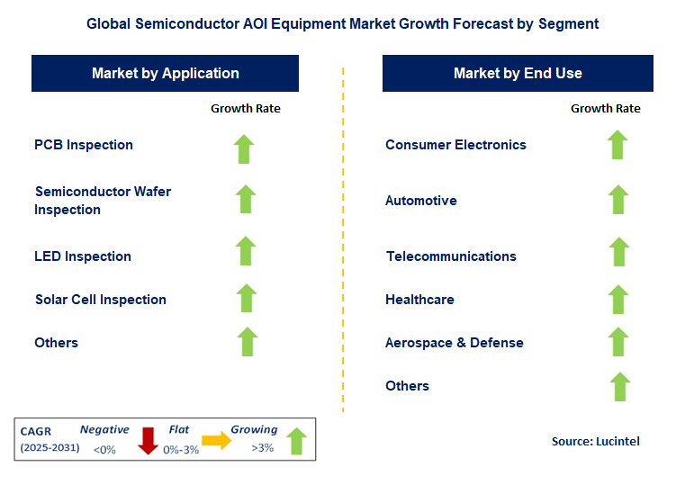
• Lucintel forecasts that, within the application category, PCB inspection is expected to witness the highest growth over the forecast period.
• Within the end use category, consumer electronic is expected to witness the highest growth.
• In terms of region, APAC is expected to witness the highest growth over the forecast period. Gain valuable insights for your business decisions with our comprehensive 150+ page report. Sample figures with some insights are shown below.
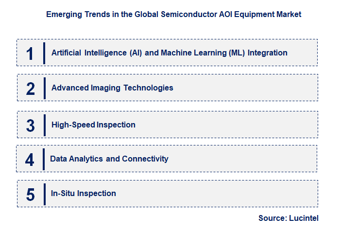
• Artificial Intelligence (AI) and Machine Learning (ML) Integration: AOI systems are increasingly incorporating AI and ML algorithms for automated defect classification and prediction. AI-powered systems can learn to identify subtle defects more accurately and efficiently than traditional rule-based systems. This improves defect detection rates, reduces false positives, and accelerates the inspection process.
• Advanced Imaging Technologies: AOI systems are adopting advanced imaging technologies, such as hyperspectral imaging, 3D imaging, and multi-view imaging, to capture more comprehensive information about wafer and chip surfaces. These technologies enable the detection of a wider range of defects, including surface scratches, particles, and structural anomalies. Enhanced imaging capabilities improve defect detection accuracy and provide more detailed defect characterization.
• High-Speed Inspection: As wafer and chip sizes increase, the need for faster inspection speeds becomes more critical. AOI systems are being developed with improved image acquisition and processing capabilities to increase throughput without compromising detection accuracy. High-speed inspection reduces inspection time, improves production efficiency, and enables faster time-to-market.
• Data Analytics and Connectivity: AOI systems are generating vast amounts of data, which can be used to optimize manufacturing processes and improve overall yield. AOI systems are being integrated with data analytics platforms and manufacturing execution systems (MES) to enable real-time monitoring of defect trends and proactive process adjustments. Data analytics and connectivity are essential for improving process control and maximizing production efficiency.
• In-Situ Inspection: In-situ inspection, which involves integrating AOI capabilities directly into process equipment, is gaining traction. In-situ inspection allows for real-time defect detection during various manufacturing steps, enabling immediate corrective actions and preventing the propagation of defects. This approach improves process control, reduces scrap rates, and enhances overall yield. These trends are collectively reshaping the semiconductor AOI equipment market by driving innovation, improving detection capabilities, and enhancing data analysis. They are leading to the development of more intelligent, faster, and more integrated AOI systems, crucial for meeting the evolving demands of semiconductor manufacturing and enabling the production of increasingly complex and high-performance chips. The future of the AOI market lies in continuous innovation and a strong focus on data-driven process optimization.
• AI-Powered Defect Detection: AOI systems are increasingly integrating artificial intelligence (AI) and machine learning (ML) algorithms for automated defect classification and prediction. AI-powered systems can learn to identify subtle defects more accurately and efficiently than traditional rule-based systems, reducing false positives and accelerating the inspection process. This leads to improved defect detection rates, reduced human intervention, and faster time-to-market.
• Advanced Imaging Technologies: AOI systems are adopting advanced imaging technologies, such as hyperspectral imaging, 3D imaging, and multi-view imaging, to capture more comprehensive information about wafer and chip surfaces. These technologies enable the detection of a wider range of defects, including surface scratches, particles, and structural anomalies, which may be missed by traditional 2D imaging. Enhanced imaging improves defect detection accuracy and provides more detailed defect characterization.
• High-Speed Inspection Systems: As wafer and chip sizes increase, the need for faster inspection speeds becomes more critical. AOI systems are being developed with improved image acquisition and processing capabilities to increase throughput without compromising detection accuracy. High-speed inspection reduces inspection time, improves production efficiency, and enables faster time-to-market for semiconductor devices.
• Data Analytics and Cloud Connectivity: AOI systems are generating vast amounts of data, which can be used to optimize manufacturing processes and improve overall yield. AOI systems are being integrated with data analytics platforms and cloud-based manufacturing execution systems (MES) to enable real-time monitoring of defect trends and proactive process adjustments. Data analytics and connectivity are essential for improving process control and maximizing production efficiency.
• In-Situ Inspection Capabilities: In-situ inspection, which involves integrating AOI capabilities directly into process equipment, is gaining traction. In-situ inspection allows for real-time defect detection during various manufacturing steps, enabling immediate corrective actions and preventing the propagation of defects. This approach improves process control, reduces scrap rates, and enhances overall yield by catching issues early. These developments are collectively reshaping the semiconductor AOI equipment market by driving innovation, improving detection capabilities, and enhancing data analysis. They are leading to the development of more intelligent, faster, and more integrated AOI systems, crucial for meeting the evolving demands of semiconductor manufacturing and enabling the production of increasingly complex and high-performance chips. The future of the AOI market lies in continuous innovation and a strong focus on data-driven process optimization.
• Advanced Node Manufacturing: The fabrication of advanced semiconductor nodes (e.g., 5nm and below) requires extremely precise and sensitive defect detection. This presents a significant growth opportunity for AOI equipment manufacturers to develop specialized systems that can detect increasingly subtle defects on these delicate and complex structures. Advanced node manufacturing demands innovative imaging and AI-powered analysis to ensure high yields.
• 3D NAND Flash Memory Fabrication: The increasing demand for 3D NAND flash memory is driving the need for advanced AOI solutions capable of inspecting the complex vertical structures of these devices. Developing specialized AOI systems optimized for 3D NAND processing offers a substantial growth opportunity. Precise defect detection is crucial during the various steps of 3D NAND fabrication, making specialized AOI essential for achieving high yields.
• Advanced Packaging Technologies: Advanced packaging technologies, such as fan-out wafer-level packaging (FOWLP) and 2.5D/3D integration, require high-precision inspection to ensure reliable device performance. AOI systems play a critical role in detecting defects in these advanced packages. Developing specialized AOI systems for these applications offers a significant growth opportunity as advanced packaging becomes more prevalent.
• Silicon Photonics Inspection: The growing adoption of silicon photonics in high-speed data communication and other applications is creating a demand for specialized AOI equipment. Silicon photonics devices have intricate structures and require precise inspection to ensure proper functionality. Developing AOI systems tailored for silicon photonics inspection presents a lucrative growth opportunity.
• Wafer Level Testing and Sort: As wafer level testing becomes more prevalent, the need for efficient and precise defect inspection and die sorting increases. AOI systems can be used to identify defective dies before packaging, improving overall manufacturing efficiency. Developing AOI systems optimized for wafer level testing and sort offers a growth opportunity as this approach becomes more common. These growth opportunities are collectively shaping the semiconductor AOI equipment market by driving innovation, increasing specialization, and expanding the market reach. They are leading to the development of more advanced and specialized AOI systems, which are essential for enabling the production of next-generation semiconductor devices. The future of the AOI market lies in continuous innovation and a strong focus on meeting the evolving inspection needs of the semiconductor industry.
• Viscom
• Marantz Electronics
• Nordson
• Koh Young Technology
• Test Research
• ViTrox
• PARMI
• Camtek
• SCREEN Holdings
• PEMTRON
• 2D AOI
• 3D AOI
• PCB Inspection
• Semiconductor Wafer Inspection
• LED Inspection
• Solar Cell Inspection
• Others
• North America
• Europe
• Asia Pacific
• The Rest of the World
• United States: The US market is characterized by a strong presence of established AOI equipment manufacturers and research institutions. Key trends include the development of advanced imaging technologies, such as hyperspectral and 3D imaging, the integration of artificial intelligence (AI) and machine learning for automated defect classification, and the development of AOI systems with higher throughput and improved sensitivity.
• China: China is rapidly expanding its semiconductor manufacturing capacity, leading to a surge in demand for AOI equipment. Chinese manufacturers are focusing on developing cost-effective AOI solutions to compete with international players. The market is also witnessing a growing emphasis on localization and domestic production of AOI equipment to support China's semiconductor industry growth.
• Germany: Germany has a strong tradition in precision engineering and manufacturing, which is reflected in its advanced AOI technologies. German companies are focusing on developing high-precision AOI systems with improved optical performance and image processing capabilities. The market is also seeing a growing emphasis on data analytics and integration with other manufacturing execution systems (MES).
• India: The Indian semiconductor industry is at a nascent stage but is expected to grow rapidly in the coming years. The Indian government is promoting initiatives to attract semiconductor manufacturing investments, which will drive the demand for AOI equipment. Indian manufacturers are focusing on developing cost-effective and reliable AOI solutions to cater to the growing domestic market.
• Japan: Japan is a leading player in the semiconductor equipment market, with a strong focus on innovation and quality. Japanese companies are developing cutting-edge AOI technologies with advanced defect detection capabilities and high throughput. The market is also seeing a growing emphasis on minimizing false positives and ensuring high accuracy in AOI systems to meet the stringent requirements of advanced semiconductor processes.

• Viscom
• Marantz Electronics
• Nordson
• Koh Young Technology
• Test Research
• ViTrox
• PARMI
• Camtek
• SCREEN Holdings
• PEMTRON Q5. Which semiconductor AOI equipment market segment will be the largest in future? Answer: Lucintel forecasts that, within the application category, PCB inspection is expected to witness the highest growth over the forecast period. Q6. In semiconductor AOI equipment market, which region is expected to be the largest in next 5 years? Answer: In terms of region, APAC is expected to witness the highest growth over the forecast period. Q7. Do we receive customization in this report? Answer: Yes, Lucintel provides 10% customization without any additional cost.


Choose a license that fits your team. Instant PDF delivery.
Prices exclude taxes. Instant delivery. Custom licensing available on request.
Market Report · July 24, 2026
Market Report · July 20, 2026
Market Report · July 20, 2026
Trusted partner for strategic intelligence and business growth


Receive a complimentary market analysis tailored to your industry. Our analysts will identify key growth opportunities and competitive dynamics specific to your business.

Market size, growth rate, and key trend analysis for your specific sector.

Top competitor positioning and market share analysis.

Strategic recommendations backed by data-driven insights.
Get curated market intelligence and competitive moves straight to your inbox.
By subscribing, you agree to receive our monthly insights. Unsubscribe anytime.
Receive a complimentary market analysis tailored to your industry. Our analysts will identify key growth opportunities and competitive dynamics specific to your business.
Market size, growth rate, and key trend analysis for your specific sector.
Top competitor positioning and market share analysis.
Strategic recommendations backed by data-driven insights.
Get curated market intelligence, emerging trends, and competitive moves straight to your inbox each month.
By subscribing, you agree to receive our monthly insights. Unsubscribe anytime.
We'll send your sample report shortly.