
Market Report · July 29, 2026

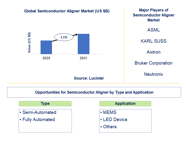
Key data points: The growth forecast = 3.1% annually for the next 7 years. Scroll below to get more insights. This market report covers trends, opportunities and forecasts in semiconductor aligner market to 2031 by type (semi-automated and fully automated), application (MEMS, LED device, and others), and region (North America, Europe, Asia Pacific, and the Rest of the World)
We'll send your sample report shortly.
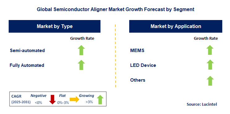
• Lucintel forecasts that, within the type category, semi-automated is expected to witness higher growth over the forecast period.
• Within the application category, MEMS is expected to witness higher growth.
• In terms of region, APAC is expected to witness the highest growth over the forecast period.
• Extreme Ultraviolet (EUV) Lithography: EUV lithography is essential for manufacturing the most advanced chips with feature sizes below 7nm. EUV aligners utilize extremely short wavelengths of light to create these tiny features, requiring highly specialized optics and vacuum systems. This trend is driving significant investment in EUV technology and shaping the high-end segment of the aligner market. The success of EUV lithography is crucial for Moore's Law to continue.
• High-Throughput Systems: Increasing wafer throughput is essential for reducing manufacturing costs and meeting the growing demand for chips. Aligner manufacturers are developing high-throughput systems that can process more wafers per hour without compromising accuracy. This involves optimizing stage movement, improving exposure systems, and incorporating advanced automation. This trend directly impacts the cost-effectiveness of chip manufacturing.
• Advanced Overlay Accuracy: Overlay accuracy, the precise alignment of successive layers during the lithography process, is critical for device performance. As feature sizes shrink, even tiny misalignments can lead to device failure. The trend is towards developing aligners with significantly improved overlay accuracy through advanced metrology and control systems. This is crucial for achieving high device yields and performance.
• Integration of Metrology and Automation: Integrating metrology tools directly into aligners allows for real-time monitoring and correction of alignment errors. This closed-loop control system improves overlay accuracy and reduces the need for separate metrology steps. Furthermore, incorporating advanced automation features, such as automated wafer handling, increases throughput and reduces human error.
• Cost-Effective Solutions for Mature Nodes: While EUV lithography dominates the leading-edge segment, there is still a significant demand for cost-effective aligners for manufacturing chips at mature nodes. Manufacturers are focusing on developing more affordable aligner solutions for these applications, often leveraging existing technologies and optimizing manufacturing processes. This ensures the continued viability of manufacturing chips for a wide range of applications.
These emerging trends are reshaping the semiconductor aligner market by driving innovation in lithography technologies, improving manufacturing efficiency, and enabling the production of increasingly complex chips. The focus on EUV lithography, high-throughput systems, advanced overlay accuracy, metrology integration, and cost-effective solutions is transforming the market landscape. The ability to meet the stringent requirements of advanced chip manufacturing while also controlling costs will be crucial for success in this highly competitive market.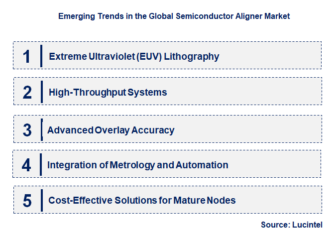
• Continued Refinement of EUV Lithography: Extreme ultraviolet (EUV) lithography remains crucial for manufacturing the most advanced chips. Recent developments focus on improving EUV source power, enhancing optics for higher resolution, and refining stage control for greater overlay accuracy. These advancements are directly enabling the production of chips with ever-smaller features, pushing the limits of Moore's Law.
• Increased Emphasis on High-NA EUV: To continue scaling chip density, the industry is transitioning to High-NA EUV lithography. This requires significantly more complex optics and stage systems, posing a major engineering challenge. Recent developments are focused on overcoming these hurdles, paving the way for future generations of chips with even higher performance.
• Development of Advanced Metrology Tools: Integrated metrology tools are becoming increasingly important for real-time monitoring and correction of alignment errors. Recent developments include incorporating advanced sensors and data analytics to improve overlay accuracy and process control. This integration reduces the need for separate metrology steps and enhances overall manufacturing efficiency.
• Focus on Heterogeneous Integration Solutions: As chip design becomes more complex, heterogeneous integration, combining different chiplets into a single package, is gaining importance. Recent developments include the development of aligners specifically designed for these advanced packaging processes, ensuring precise alignment of the different chiplets.
• Improvements in Stage Speed and Automation: Increasing wafer throughput is crucial for reducing manufacturing costs. Recent developments are focused on improving stage speed and incorporating more sophisticated automation features, such as automated wafer handling and alignment routines. These improvements enhance productivity and reduce the time required to manufacture chips.
These recent developments are significantly impacting the semiconductor aligner market by enabling the production of more advanced chips with higher density and performance. The continued refinement of EUV lithography, the development of High-NA EUV, the integration of advanced metrology, the focus on heterogeneous integration, and improvements in stage speed and automation are all contributing to the evolution of this critical market. These advancements are pushing the boundaries of semiconductor technology and driving the continued progress of the electronics industry.• Advanced Logic and Memory Devices: The relentless pursuit of Moore's Law drives the demand for cutting-edge aligners capable of manufacturing the most advanced logic and memory chips. This includes continuous refinement of EUV lithography and the development of High-NA EUV systems. Companies that can deliver the required precision and throughput for these leading-edge applications will capture significant market share. This directly impacts the performance and density of future generations of processors and memory chips.
• High-Bandwidth Memory (HBM) and 3D Packaging: High-bandwidth memory and 3D packaging technologies are crucial for increasing memory capacity and performance. Aligners play a key role in these advanced packaging processes, requiring high overlay accuracy and specialized handling capabilities. Developing aligners specifically designed for HBM and 3D packaging offers a substantial growth opportunity. This enables the creation of more powerful and efficient computing systems.
• Photonics and Integrated Optics: The growing field of photonics, using light for information processing, presents a new growth opportunity for aligner manufacturers. Aligners are needed to precisely pattern optical waveguides and other photonic structures. Adapting aligner technology for the unique requirements of photonics, such as handling different substrate materials, can open up a new market segment. This will accelerate the development of integrated optical circuits and devices.
• MEMS and Sensors: Microelectromechanical systems (MEMS) and sensors are used in a wide range of applications, from automotive to consumer electronics. Aligners are essential for manufacturing these devices, requiring specialized features such as handling non-silicon substrates and patterning complex microstructures. Developing cost-effective aligner solutions for MEMS and sensor manufacturing offers a valuable growth opportunity. This will improve the performance and reduce the cost of various sensor-based technologies.
• Advanced Packaging and Heterogeneous Integration: Heterogeneous integration, combining different chiplets into a single package, is becoming increasingly important for achieving higher system performance. Aligners are used in various steps of these advanced packaging processes, requiring high overlay accuracy and the ability to handle different chip sizes and materials. Developing aligners optimized for heterogeneous integration is crucial for enabling this technology. This will lead to more complex and integrated systems-on-a-chip.
These strategic growth opportunities are significantly impacting the semiconductor aligner market by driving innovation in lithography technologies and expanding their applications across a wider range of devices. The demand for advanced logic and memory, the rise of HBM and 3D packaging, the growth of photonics, the proliferation of MEMS and sensors, and the increasing importance of heterogeneous integration are all contributing to the evolution of this critical market. Companies that can anticipate and effectively address the specific needs of these diverse applications are poised for success in this dynamic landscape.• ASML
• KARL SUSS
• Aixtron
• Bruker Corporation
• Neutronix
• Vistec Electron Beam
• EV Group
• Canon
• DNK
• MIKASA
• Semi-automated
• Fully Automated
• MEMS
• LED Device
• Others
• North America
• Europe
• Asia Pacific
• The Rest of the World
• United States: The US has a strong presence in the semiconductor aligner market, with companies like ASML (though headquartered in the Netherlands, they have significant US operations and influence) playing a leading role. Recent developments include the refinement of extreme ultraviolet (EUV) lithography aligners, which are essential for manufacturing the most advanced chips. US companies are also focusing on developing advanced metrology tools integrated with aligners to improve overlay accuracy and process control. Furthermore, there's a growing emphasis on developing solutions for heterogeneous integration and advanced packaging.
• China: China is rapidly expanding its domestic semiconductor manufacturing capacity, leading to a surge in demand for aligners. Chinese manufacturers are focusing on developing competitive aligners for both traditional and advanced lithography processes. While still behind global leaders in terms of the most advanced EUV technology, Chinese companies are making strides in developing deep ultraviolet (DUV) lithography equipment and improving the performance and reliability of their aligners. Government support and investment are playing a key role in this growth.
• Germany: Germany has a long tradition of excellence in optics and precision engineering, which is crucial for the development of advanced aligners. German companies are focusing on developing high-precision optical systems and mechanical components for aligners. They are also specializing in developing aligners for niche applications, such as MEMS manufacturing and advanced packaging. Close collaboration between research institutions and industry is a hallmark of the German approach.
• India: The Indian semiconductor industry is still in its nascent stages, and the demand for aligners is currently met primarily through imports. However, as India aims to become a more significant player in the global semiconductor market, there is growing interest in establishing domestic aligner manufacturing capabilities. The focus is on developing more affordable and accessible aligners suitable for the needs of emerging Indian chip manufacturers. Government initiatives are encouraging investment in this area.
• Japan: Japan has a long-standing presence in the semiconductor equipment market, including aligners. Japanese companies are known for their expertise in precision engineering and high-quality manufacturing. They are focusing on developing highly reliable and accurate aligners for advanced lithography processes. Japanese manufacturers are also emphasizing the integration of advanced metrology and automation capabilities into their aligner systems to improve overall manufacturing efficiency.
• ASML
• KARL SUSS
• Aixtron
• Bruker Corporation
• Neutronix
• Vistec Electron Beam
• EV Group
• Canon
• DNK
• MIKASA
Q5. Which semiconductor aligner market segment will be the largest in future?

Choose a license that fits your team. Instant PDF delivery.
Prices exclude taxes. Instant delivery. Custom licensing available on request.
Market Report · July 29, 2026
Market Report · July 20, 2026
Market Report · July 20, 2026
Trusted partner for strategic intelligence and business growth


Receive a complimentary market analysis tailored to your industry. Our analysts will identify key growth opportunities and competitive dynamics specific to your business.

Market size, growth rate, and key trend analysis for your specific sector.

Top competitor positioning and market share analysis.

Strategic recommendations backed by data-driven insights.
Get curated market intelligence and competitive moves straight to your inbox.
By subscribing, you agree to receive our monthly insights. Unsubscribe anytime.
Receive a complimentary market analysis tailored to your industry. Our analysts will identify key growth opportunities and competitive dynamics specific to your business.
Market size, growth rate, and key trend analysis for your specific sector.
Top competitor positioning and market share analysis.
Strategic recommendations backed by data-driven insights.
Get curated market intelligence, emerging trends, and competitive moves straight to your inbox each month.
By subscribing, you agree to receive our monthly insights. Unsubscribe anytime.
We'll send your sample report shortly.