
Market Report · July 17, 2026

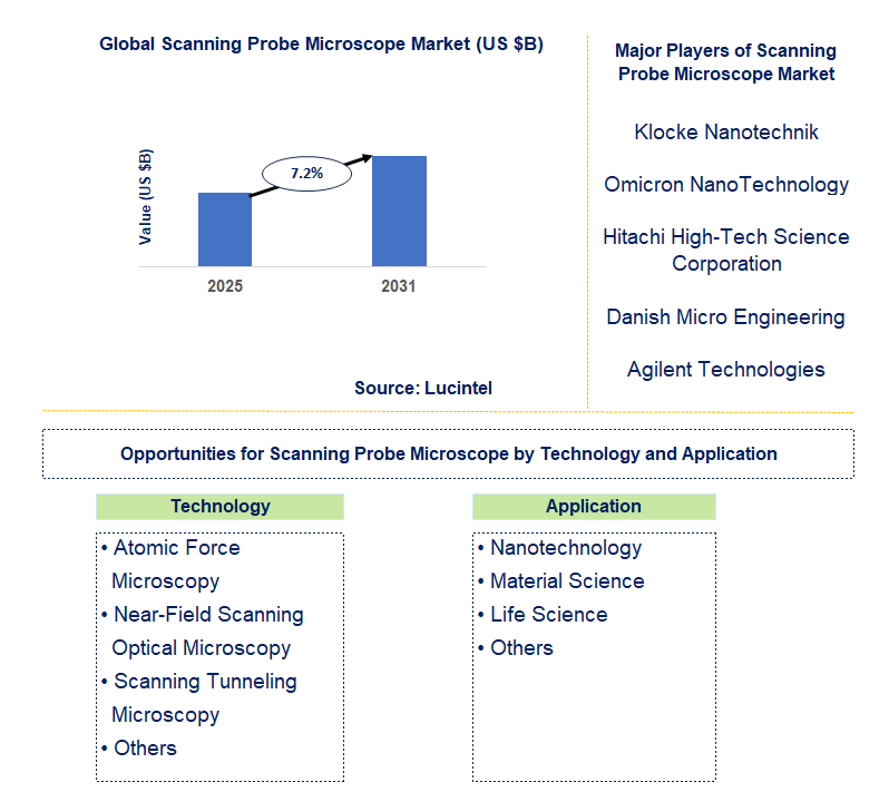
Key data points: The growth forecast = 7.2% annually for the next 7 years. Scroll below to get more insights. This market report covers trends, opportunities and forecasts in scanning probe microscope market to 2031 by technology (atomic force microscopy, near-field scanning optical microscopy, scanning tunneling microscopy, and others), application (nanotechnology, material science, life science, and others), and region (North America, Europe, Asia Pacific, and the Rest of the World)
We'll send your sample report shortly.
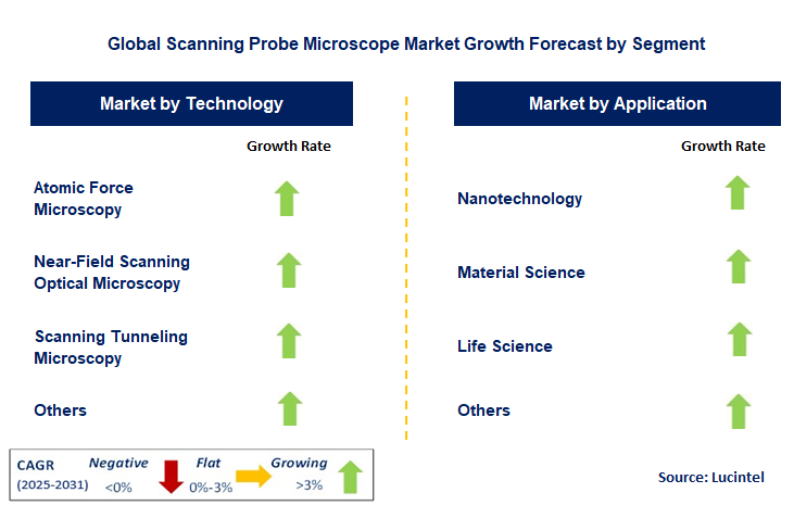
• Lucintel forecasts that, within the technology category, atomic force microscopy is expected to witness the highest growth over the forecast period.
• Within the application category, life science is expected to witness the highest growth.
• In terms of region, APAC is expected to witness the highest growth over the forecast period. Gain valuable insights for your business decisions with our comprehensive 150+ page report. Sample figures with some insights are shown below.
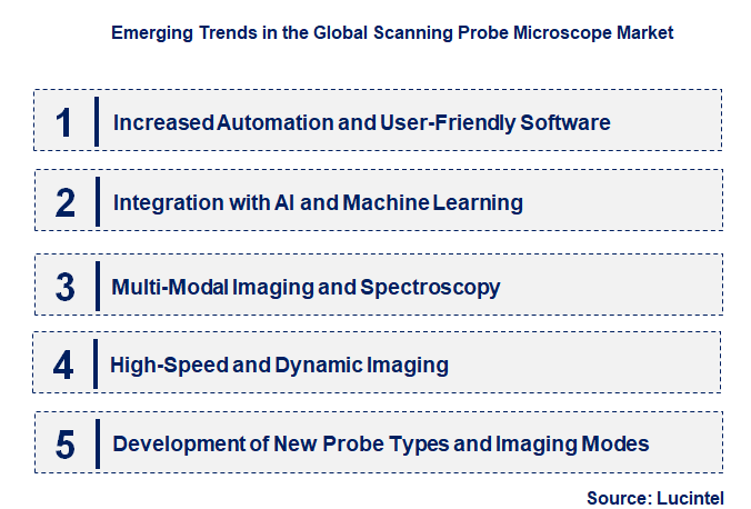
• Increased Automation and User-Friendly Software: This trend focuses on developing SPM systems with enhanced automation features and intuitive software interfaces. The goal is to simplify operation, reduce the need for highly specialized personnel, and accelerate data acquisition and analysis, making SPM technology more accessible to a broader range of researchers and industrial users.
• Integration with AI and Machine Learning: The incorporation of artificial intelligence and machine learning algorithms into SPM workflows is a significant trend. AI enhances image processing, automates data analysis, and can even predict optimal scanning parameters, leading to faster research cycles, improved data accuracy, and the ability to extract deeper insights from complex nanoscale data.
• Multi-Modal Imaging and Spectroscopy: There’s a growing trend to integrate SPM techniques with other analytical methods, such as Raman spectroscopy, optical microscopy, and electron microscopy. This multi-modal approach provides comprehensive information about a sample’s physical, chemical, and optical properties simultaneously, offering a more complete characterization at the nanoscale.
• High-Speed and Dynamic Imaging: Developments are pushing for significantly faster imaging speeds in SPM, enabling real-time visualization of dynamic processes at the nanoscale. This is crucial for studying transient phenomena in materials science, chemical reactions, and biological systems, opening new avenues for understanding fundamental processes.
• Development of New Probe Types and Imaging Modes: Continuous innovation in probe design and the creation of novel imaging modes are expanding the capabilities of SPM. This includes probes for specific functionalities (e.g., electrical, magnetic, thermal measurements) and new modes that offer enhanced sensitivity, resolution, or the ability to probe specific material properties, driving new applications. These emerging trends are profoundly reshaping the scanning probe microscope market by making SPM technology more powerful, accessible, and versatile. The focus on automation, intelligent data analysis, multi-dimensional characterization, and dynamic studies is driving innovation and expanding the scientific and industrial impact of SPM.
• Launch of High-Speed AFM Systems: A significant development is the commercial release of new high-speed Atomic Force Microscope (AFM) systems. For instance, some manufacturers have launched AFMs capable of imaging at 50 frames per second, enabling real-time visualization of dynamic biological processes and material transformations, a breakthrough for understanding nanoscale kinetics.
• Advancements in High-Sensitivity SPM: Recent innovations include the development of SPM systems with newly designed high-sensitivity optical heads. These improvements, seen in products like Hitachi High-Tech’s AFM100 Pro, enhance the ability to measure physical properties at atomic and molecular scales, providing unprecedented detail for material characterization.
• Integration of AI for Automated Analysis: Leading SPM manufacturers are increasingly integrating artificial intelligence and machine learning algorithms into their software platforms. This development automates complex image acquisition, processing, and data analysis tasks, significantly reducing research time and enhancing the accuracy of nanoscale measurements.
• Development of Ultrafast Time-Resolved STM: Breakthroughs in Scanning Tunneling Microscopy (STM) include the development of ultrafast time-resolved STM systems, achieved through collaborations between companies and academic institutions. These systems combine optical pump-probe methods with STM, allowing for the study of carrier dynamics at the nanoscale with unprecedented temporal resolution.
• Expanded Multi-Modal Capabilities: Recent developments emphasize the integration of SPM with other analytical techniques, such as Raman spectroscopy and optical microscopy, within a single system. This multi-modal approach provides comprehensive information about a sample’s structural, chemical, and electrical properties simultaneously, accelerating research and development. These key developments are profoundly impacting the scanning probe microscope market by enhancing imaging speed, sensitivity, and analytical capabilities. The focus on real-time dynamics, automated analysis, and comprehensive multi-modal characterization is driving innovation and solidifying the SPM’s role as a cornerstone of nanotechnology and materials science.
• Semiconductor and Electronics Industry: This is a major growth driver. Opportunities lie in developing SPM systems for quality control, failure analysis, and characterization of advanced semiconductor components and nanoelectronics devices. Emphasize high-resolution imaging for defect detection and precise measurement of thin films and complex architectures to meet miniaturization demands.
• Nanomaterials Science and Research: The burgeoning field of nanomaterials, including graphene, quantum dots, and nanotubes, presents significant opportunities. Develop SPM solutions for characterizing the structural, electrical, mechanical, and magnetic properties of these novel materials, crucial for their development and integration into new technologies.
• Life Sciences and Biomedical Applications: SPM offers unique insights into biological samples at the cellular and molecular level. Opportunities include developing SPM for studying cell mechanics, protein interactions, DNA structures, and drug delivery systems. Focus on capabilities like imaging in liquid environments and gentle force control for biological samples.
• Academic and Government Research Institutions: These institutions are fundamental to scientific discovery and receive substantial funding for advanced research. Strategic growth involves providing versatile, high-performance SPM systems that can address a wide range of research questions across physics, chemistry, materials science, and biology, fostering innovation and technological breakthroughs.
• Quality Control and Industrial R&D: Beyond fundamental research, there’s a growing opportunity for SPM in industrial quality control and applied R&D across various sectors (e.g., automotive, aerospace, chemicals). Develop robust, user-friendly SPM systems for material characterization, surface roughness analysis, and defect inspection in manufacturing processes. These strategic growth opportunities are impacting the scanning probe microscope market by driving product specialization and expanding its application beyond traditional research. By addressing the unique demands of high-growth industries and critical research areas, the market can achieve broader penetration and solidify the indispensable role of SPM in the nanoscale revolution.
• Klocke Nanotechnik
• Omicron NanoTechnology
• Hitachi High-Tech Science Corporation
• Danish Micro Engineering
• Agilent Technologies
• Atomic Force Microscopy
• Near-Field Scanning Optical Microscopy
• Scanning Tunneling Microscopy
• Others
• Nanotechnology
• Material Science
• Life Science
• Others
• North America
• Europe
• Asia Pacific
• The Rest of the World
• United States: The US market for SPM is highly innovative, driven by robust funding in academic research and a strong semiconductor industry. Recent developments include increased integration of AI for automated image analysis and the commercialization of high-speed AFM systems, facilitating real-time visualization of dynamic processes crucial for advanced research.
• China: China’s SPM market is rapidly expanding, fueled by significant government investments in nanotechnology and materials science research. Local manufacturers are improving capabilities, while increased adoption in electronics and life sciences, along with a focus on indigenous innovation, are driving the demand for advanced nanoscale imaging tools.
• Germany: Germany’s SPM market emphasizes precision engineering and high-performance instrumentation. Recent developments focus on integrating SPM with other analytical techniques like Raman spectroscopy, enhancing multi-modal characterization capabilities. A strong research infrastructure and collaborations with leading manufacturers continue to drive market advancements.
• India: India’s SPM market is growing, driven by increasing government initiatives and funding for research institutions in nanotechnology and materials science. The market is seeing a rise in demand for advanced microscopy to support drug discovery, materials development, and academic research, indicating a developing but promising landscape.
• Japan: Japan’s SPM market is characterized by a strong presence of key manufacturers and a focus on cutting-edge technology. Recent developments include the launch of high-sensitivity AFM systems and ultrafast time-resolved STM systems, demonstrating a commitment to pushing the boundaries of nanoscale measurement and dynamic imaging.


• Klocke Nanotechnik
• Omicron NanoTechnology
• Hitachi High-Tech Science Corporation
• Danish Micro Engineering
• Agilent Technologies Q5. Which scanning probe microscope market segment will be the largest in future? Answer: Lucintel forecasts that, within the technology category, atomic force microscopy is expected to witness the highest growth over the forecast period. Q6. In scanning probe microscope market, which region is expected to be the largest in next 5 years? Answer: In terms of region, APAC is expected to witness the highest growth over the forecast period. Q7. Do we receive customization in this report? Answer: Yes, Lucintel provides 10% customization without any additional cost.


Choose a license that fits your team. Instant PDF delivery.
Prices exclude taxes. Instant delivery. Custom licensing available on request.
Market Report · July 17, 2026
Market Report · July 16, 2026
Market Report · July 10, 2026
Trusted partner for strategic intelligence and business growth


Receive a complimentary market analysis tailored to your industry. Our analysts will identify key growth opportunities and competitive dynamics specific to your business.

Market size, growth rate, and key trend analysis for your specific sector.

Top competitor positioning and market share analysis.

Strategic recommendations backed by data-driven insights.
Get curated market intelligence and competitive moves straight to your inbox.
By subscribing, you agree to receive our monthly insights. Unsubscribe anytime.
Receive a complimentary market analysis tailored to your industry. Our analysts will identify key growth opportunities and competitive dynamics specific to your business.
Market size, growth rate, and key trend analysis for your specific sector.
Top competitor positioning and market share analysis.
Strategic recommendations backed by data-driven insights.
Get curated market intelligence, emerging trends, and competitive moves straight to your inbox each month.
By subscribing, you agree to receive our monthly insights. Unsubscribe anytime.
We'll send your sample report shortly.