
Market Report · July 24, 2026

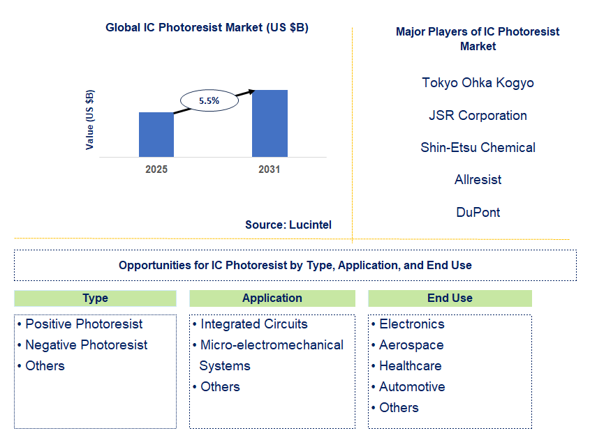
Key data points: The growth forecast = 5.5% annually for the next 7 years. Scroll below to get more insights. This market report covers trends, opportunities and forecasts in IC photoresist market to 2031 by type (positive photoresist, negative photoresist, and others), application (integrated circuits, micro-electromechanical systems, and others), end use (electronics, aerospace, healthcare, automotive, and others), and region (North America, Europe, Asia Pacific, and the Rest of the World)
We'll send your sample report shortly.
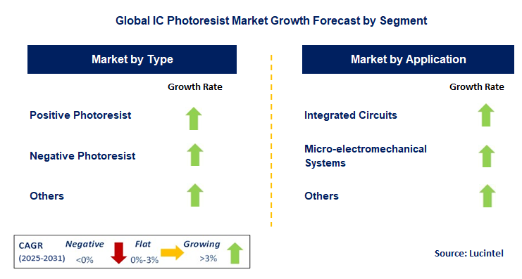
• Lucintel forecasts that, within the type category, positive photoresist is expected to witness higher growth over the forecast period.
• Within the application category, integrated circuit is expected to witness higher growth.
• In terms of region, APAC is expected to witness the highest growth over the forecast period. Gain valuable insights for your business decisions with our comprehensive 150+ page report. Sample figures with some insights are shown below.
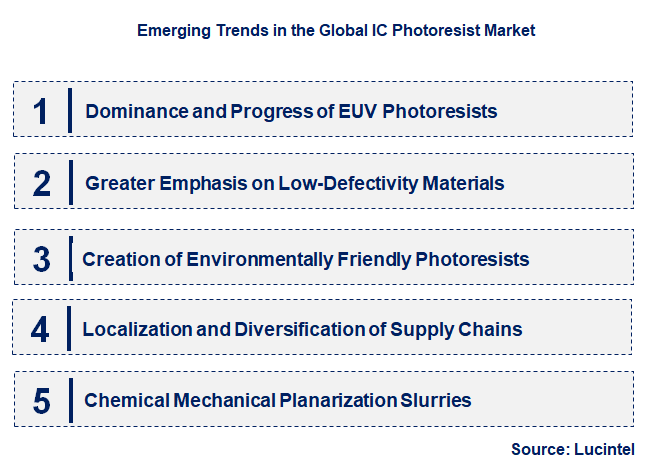
• Dominance and Progress of EUV Photoresists: Extreme Ultraviolet (EUV) lithography is currently essential for the production of advanced integrated circuits at sub-7nm nodes, and thus EUV photoresists are the most important upcoming trend. Such photoresists are engineered to be extremely sensitive to EUV radiation so that they can be used to pattern extremely fine features with excellent fidelity. Ongoing research is directed towards enhancing their resolution, line edge roughness, and defectivity, along with new chemistries to match the requirements of subsequent smaller nodes.
• Greater Emphasis on Low-Defectivity Materials: As semiconductor sizes decrease, even minor defects in the photoresist layer can result in disastrous failures in the finished chip. As a result, there is great emphasis on creating ultra-low defectivity photoresist products. This entails thorough purification steps, sophisticated filtration methods, and better formulation control to reduce impurities and particles. The result is an increased manufacturing yield for chipmakers and lower costs of production for complicated integrated circuits.
• Creation of Environmentally Friendly Photoresists: Increased environmental awareness and more stringent regulations are pushing the trend towards greener photoresists. This involves investigation into lower VOC emissions, less hazardous chemical content, and better biodegradability. The goal is to produce photoresists safer for employees and with a reduced environmental impact during their entire lifecycle, from production to end-of-life disposal.
• Localization and Diversification of Supply Chains: Geopolitical tensions and historical supply chain disruptions highlighted the weakness of a highly concentrated photoresist supply chain. A growing trend is the strategic push by nations such as China and the United States to localize and diversify their photoresist manufacturing capabilities. It includes huge investments in local manufacturing facilities and R&D, with a goal of diminishing dependence on a limited number of global suppliers and bolstering national semiconductor security.
• Chemical Mechanical Planarization Slurries: The behavior of photoresists is highly influenced by ancillary, or complement, materials such as developers, removers, and anti-reflective coatings. A new trend is the co-optimization and co-development of these ancillaries to coexist with cutting-edge photoresists in a perfectly compatible manner, even further improving patterning precision and process control. New developments in Chemical Mechanical Planarization (CMP) slurries that polish wafers are also vital in establishing flat surfaces required for multi-layer chip structures. These new trends are all reinforcing one another to collectively transform the IC photoresist industry in the direction of further advanced, sustainable, and secure materials. EUV photoresists' dominance, low defectivity's relentless pursuit, environmental friendliness' pursuit, the strategic drive for localization of the supply chain, and ancillaries' synergistic development are all reinforcing a very dynamic, innovative environment. These trends are essential to support the next generation of semiconductor technology.
• Advancement in Extreme Ultraviolet Photoresist Performance: One of the biggest recent breakthroughs has been significant improvement in EUV photoresist performance. Producers have greatly enhanced their resolution, sensitivity, and defectivity properties. Some of these developments have involved creating new polymer platforms, photoacid generators, and quenchers that are more effective at absorbing EUV light and forming accurate patterns. All these developments are essential for mass production of chips at 5nm, 3nm, and even below those process nodes, taking chip miniaturization to new dimensions.
• Improved Resolution and Line Edge Roughness Control: Recent research has been centered on increasing the resolution and managing line edge roughness (LER) in photoresists. Production of finer patterns with smooth, uniform edges is crucial to bettering chip performance and yield. Novel photoresist chemistries and processing methods, such as sophisticated baking and development protocols, are being utilized to reduce LER and pattern collapse, providing higher fidelity in transferred patterns onto the silicon wafer.
• Novel Material Chemistries: The industry is witnessing the development of new material chemistries for photoresists, away from conventional platforms. These involve explorations of metal-oxide resists, molecular resists, and inorganic resists, that have superior properties like increased EUV absorption, enhanced etch resistance, and enhanced pattern fidelity at ultra-small sizes. These alternative chemistries are poised to break some of the inherent limitations of organic polymer-based photoresists in future nodes.
• Expanded Automation and Quality Assurance in Manufacturing: Recent trends also involve major investments in automation and sophisticated quality control techniques in photoresist manufacturing plants. This provides ultra-high purity, consistency, and traceability of products. Automated manufacturing reduces human error and contamination, and advanced analytical methods ensure that every batch of photoresist conforms to the rigorous specifications needed for advanced semiconductor manufacturing, leading to enhanced yield and reliability for chipmakers.
• Strategic Partnerships and Joint Development Programs: There is increasing development of strategic partnerships among photoresist suppliers, lithography tool vendors (such as ASML), and top-ranked semiconductor foundries. These joint development programs are extremely important for speeding up innovation, guaranteeing material compatibility with next-generation lithography tools, and facilitating the integration of new photoresist technologies into high-volume manufacturing. These partnerships are extremely important to counteract the extremely sophisticated challenges of advanced semiconductor production. These newer developments are having a dramatically significant effect on the IC photoresist market directly by facilitating the progression of semiconductor technology. Innovation in EUV photoresist performance, an unrelenting drive for greater resolution and lower defectivity, an investigation into new chemistries, the increase of manufacturing quality, and strategic collaborative efforts by the industry are all fueling the market. These developments are critical for ongoing miniaturization and increasing performance of integrated circuits worldwide.
• Advanced Microprocessor and Logic Manufacturing: The insatiable need for higher speed and more capable logic chips and microprocessors (CPUs, GPUs) for data centers, AI, and high-performance computing is a critical growth opportunity. Such applications demand the most sophisticated lithography processes, specifically EUV, and thus state-of-the-art EUV photoresists with the highest resolution, sensitivity, and lowest defectivity. Strategic growth is in creating and delivering ultra-premium photoresists that allow the production of sub-3nm nodes, extending the transistor density limits.
• Memory Chip Manufacture (DRAM and NAND Flash): The explosive growth in demand for memory chips, particularly DRAM and NAND Flash for mobile phones, solid-state drives (SSDs), and data center storage, provides significant opportunities for growth. Although memory chips tend to use slightly less advanced lithography nodes than cutting-edge logic, their sheer scale and the complexity of 3D NAND structures create steady demand for high-performance ARF and KRF photoresists. Growth opportunities lie in the optimization of photoresists for multi-patterning methods and enhancing process windows for high-volume memory production.
• Automotive Electronics and Sensors: The high-rate development of the automotive electronics market, mainly for advanced driver-assistance systems (ADAS), infotainment, and electric vehicle (EV) components, generates a strong demand for IC photoresists. The chips need to be highly reliable and rugged, frequently produced using mature and established lithography technologies (e.g., KrF, I-line). Strategic expansion includes supplying stable and economical photoresists that satisfy the severe quality and durability needs of the automotive sector with zero defects.
• Advanced Packaging (3D-IC, Fan-Out Wafer Level Packaging): The transformation towards advanced packaging technologies, including 3D integrated circuits (3D-IC) and fan-out wafer-level packaging (FOWLP), brings about upcoming growth opportunities. These technologies necessitate special photoresists to develop complex interconnects, redistribution layers (RDLs), and through-silicon vias (TSVs). Strategic growth entails photoresist development that can provide excellent thickness uniformity, high aspect ratio patterning, and compatibility with numerous advanced packaging materials and processes.
• Optoelectronics and Micro-Electro-Mechanical Systems: The growing optoelectronics (e.g., optical sensors, LiDAR) and Micro-Electro-Mechanical Systems (MEMS) (e.g., accelerometers, gyroscopes, microphones) markets also present special growth opportunities. These applications tend to require specialized processing steps that demand specific photoresist attributes, e.g., high optical transparency for optical uses or high etch resistance for MEMS devices. Niche photoresist formulation opportunities exist for developing special photoresists suited to the specific patterning requirements of these varied and fast-developing markets. These strategic growth prospects highlight the critical role of IC photoresists throughout the semiconductor value chain. By targeting the distinctive requirements of advanced logic, high-volume memory, rigorous automotive electronics, advanced packaging complexity, and specialized optoelectronics/MEMS, photoresist suppliers can fuel innovation and capture considerable market share. This focused strategy assures continued expansion and technological dominance in the IC photoresist market.
• Tokyo Ohka Kogyo
• JSR Corporation
• Shin-Etsu Chemical
• Allresist
• DuPont
• Eteal Materials
• Jiangsu Nata Opto-electronic Material
• Fujifilm Electronic Materials
• Merck Group
• LG Chem
• Positive Photoresist
• Negative Photoresist
• Others
• Integrated Circuits
• Micro-electromechanical Systems
• Others
• North America
• Europe
• Asia Pacific
• The Rest of the World
• United States: In the United States, the IC photoresist industry is spurred by the location of large semiconductor companies and research facilities. Recent advances involve the creation of sophisticated photoresist materials for next-generation nodes, specifically EUV photoresists. Heavy investment in research and development is directed toward enhanced resolution, sensitivity, and defectivity, quite often in co-operation with equipment vendors. The aim is to facilitate next-generation chip production and insuring domestic supply chains for strategic materials.
• China: China's IC photoresist industry is growing at a fast pace, driven by the aggressive plans of the government to become independent in the production of semiconductors. Though traditionally import-dependent, Chinese manufacturers are majorly progressing in domesticating the production of different types of photoresists, such as KRF and ARF photoresists. Latest trends suggest major developments in domestic certification and winning orders from local wafer makers, which is a key step toward minimizing foreign dependence and enhancing their domestic supply chain.
• Germany: Germany is an important part of the European semiconductor value chain, and its contribution to the IC photoresist industry comes in the form of specialized chemicals firms and research initiatives. Although it is not a top photoresist manufacturing country on the East Asian level, Germany specializes in high-purity chemicals and materials science. Innovations tend to be associated with joint ventures with overseas partners, with the purpose of advancing advanced manufacturing processes and investigating new photoresist chemistries that may advance performance and sustainability.
• India: India's IC photoresist market is emerging and increasing, supported mainly by the rise in demand for electronic products and early attempts at creating a local semiconductor production ecosystem. Although at present a smaller consumer than other parts of the world, India is shifting its attention towards building semiconductor material capabilities. Emerging trends show increasing interest in photoresist chemicals, and scope to expand as the nation increases its electronics production and possibly gets into wafer fabrication.
• Japan: Japan leads the world in the IC photoresist market, with a number of key players that specialize in high-tech and high-quality materials. Current developments in Japan revolve around sustained innovation in EUV photoresists, breaking frontiers in resolution and defect control. Japanese players are spending big on R&D and increasing production capacities to keep up with the growing global demand for advanced semiconductors, especially for leading-edge logic and memory chips.


• Tokyo Ohka Kogyo
• JSR Corporation
• Shin-Etsu Chemical
• Allresist
• DuPont
• Eteal Materials
• Jiangsu Nata Opto-electronic Material
• Fujifilm Electronic Materials
• Merck Group
• LG Chem Q5. Which IC photoresist market segment will be the largest in future? Answer: Lucintel forecasts that, within the type category, positive photoresist is expected to witness higher growth over the forecast period. Q6. In IC photoresist market, which region is expected to be the largest in next 5 years? Answer: In terms of region, APAC is expected to witness the highest growth over the forecast period. Q7. Do we receive customization in this report? Answer: Yes, Lucintel provides 10% customization without any additional cost.


Choose a license that fits your team. Instant PDF delivery.
Prices exclude taxes. Instant delivery. Custom licensing available on request.
Market Report · July 24, 2026
Market Report · July 20, 2026
Market Report · July 20, 2026
Trusted partner for strategic intelligence and business growth


Receive a complimentary market analysis tailored to your industry. Our analysts will identify key growth opportunities and competitive dynamics specific to your business.

Market size, growth rate, and key trend analysis for your specific sector.

Top competitor positioning and market share analysis.

Strategic recommendations backed by data-driven insights.
Get curated market intelligence and competitive moves straight to your inbox.
By subscribing, you agree to receive our monthly insights. Unsubscribe anytime.
Receive a complimentary market analysis tailored to your industry. Our analysts will identify key growth opportunities and competitive dynamics specific to your business.
Market size, growth rate, and key trend analysis for your specific sector.
Top competitor positioning and market share analysis.
Strategic recommendations backed by data-driven insights.
Get curated market intelligence, emerging trends, and competitive moves straight to your inbox each month.
By subscribing, you agree to receive our monthly insights. Unsubscribe anytime.
We'll send your sample report shortly.