
Market Report · May 18, 2026

This market report covers trends, opportunities, and forecasts in the global hard chemical mechanical polishing pad market to 2031 by technology (silicon wafer, sic wafer, and others), application (300mm wafer, 200mm wafer, and others), and region (North America, Europe, Asia Pacific, and the Rest of the World)
We'll send your sample report shortly.
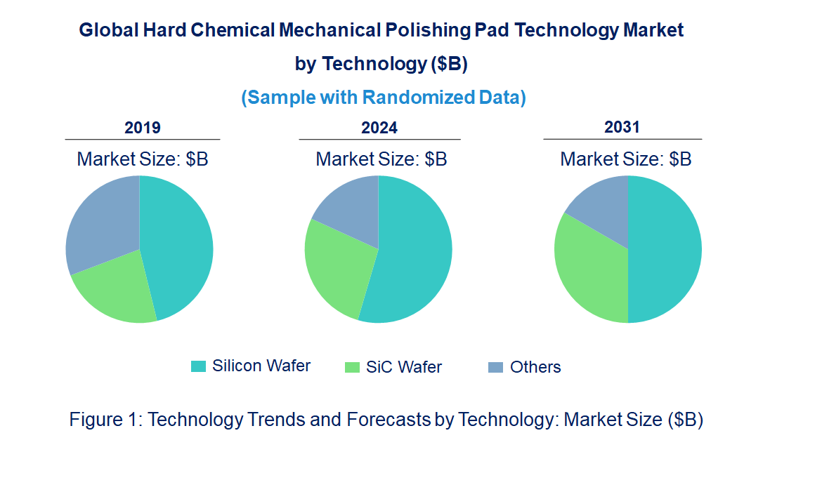
• Silicon Carbide (SiC) and Advanced Wafer Materials: The rising demand for power semiconductor devices has led to a trend toward the use of SiC wafers in chemical mechanical polishing. Since SiC is harder to polish than conventional silicon, new chemical mechanical polishing pads are being developed for advanced materials.
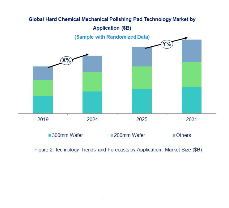
• Customization of chemical mechanical polishing Pads for Particular Wafer Sizes: While wafers are increasing in size, 300mm is now the standard, with wafer sizes being optimally customized for chemical mechanical polishing pads to help better polish larger substrates. Tailor-made pads improve the accuracy and quality of polishing, decrease defects in wafers, and increase the yield rate in semiconductor manufacturing.
• Integration of Nanomaterials for Enhanced Performance: Nanotechnology is being increasingly integrated into the design of chemical mechanical polishing pads to enhance their performance. The use of nanomaterial-infused pads delivers higher material removal rates, fewer surface defects, and improved uniformity that is essential for manufacturing next-generation high-performance semiconductors.
• Focus on Pad Longevity and Cost-Efficiency: There is a growing emphasis on developing chemical mechanical polishing pads with longer lifespans to reduce the frequency of replacement and minimize operational costs. Manufacturers are focusing on improving pad durability through advanced material science and surface treatments to ensure more cost-effective polishing processes.
• Environmental and Sustainability Concerns: As sustainability becomes a major priority for the semiconductor industry, manufacturers are focusing more on eco-friendly chemical mechanical polishing pad materials. The use of recyclable and environmentally friendly materials, as well as water-saving and low-energy processes, is expected to grow in the coming years. These trends demonstrate that the hard chemical mechanical polishing pad market is experiencing exciting technological developments. Improvements in polishing efficiency are enhancing the ability to customize advanced wafer materials and creating an environmental sustainability revolution, thereby transforming the landscape of semiconductor fabrication.
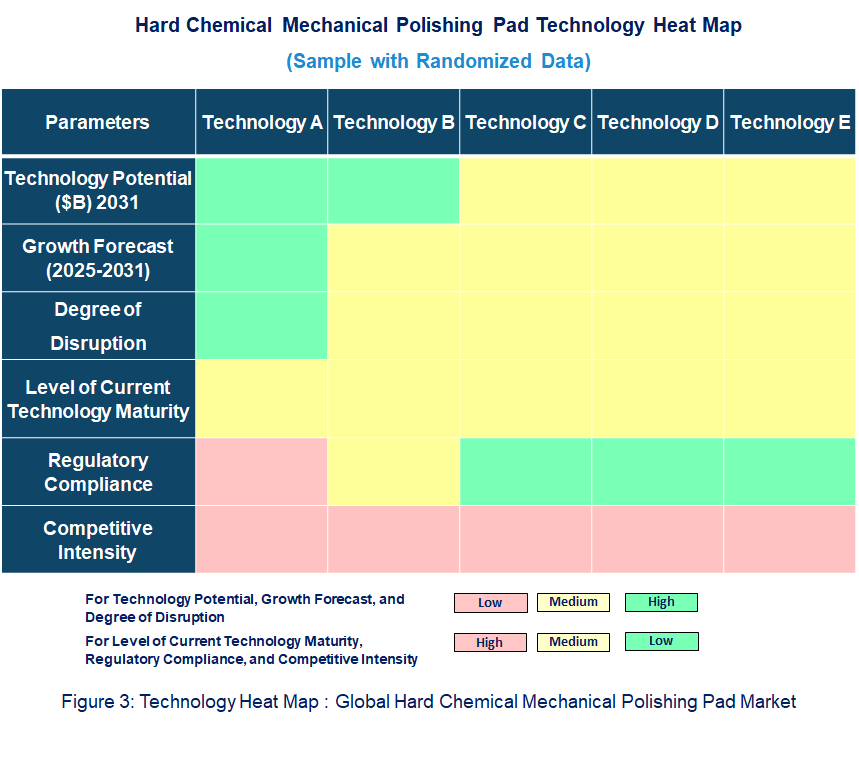
• Technology Potential: The potential of chemical mechanical polishing pad technology is vast, especially with the further miniaturization of semiconductor devices and the growing need for higher precision in the manufacturing process. Innovations in material science, including the development of advanced polyurethane-based and nanostructured pads, provide better performance in terms of pad longevity, uniformity, and reduced defects. As semiconductor nodes shrink to sub-5nm levels, the demand for advanced chemical mechanical polishing pads that can maintain high planarization performance while minimizing defects is increasing.
• Degree of Disruption: Chemical mechanical polishing pads are essential in semiconductor fabrication. Advanced technologies could have a significant impact on manufacturing efficiency, cost savings, and yield enhancement of semiconductor fabs.
• Current Technology Maturity Level: The introduction of new materials and surface treatments in chemical mechanical polishing pads may critically affect both cost and performance in semiconductor fabs. Chemical mechanical polishing pad technology is somewhat mature, with established suppliers offering reliable products. However, current research continues to focus on improving pad durability and performance for next-generation devices.
• Regulatory Compliance: Industry and Environmental Compliance: In the semiconductor industry, chemical mechanical polishing pads must comply with industry-specific standards and material safety regulations. Compliance with environmental regulations is critical, as the chemical treatments used in the chemical mechanical polishing process can impact the environment.
• DuPont: DuPont has created advanced chemical mechanical polishing pads specifically designed for SiC wafer polishing, enabling more efficient and defect-free processing of power semiconductor devices. Through their high-performance pads, which enhance yield and process efficiency, DuPont has significantly outpaced its competitors.
• CMC Materials: CMC Materials launched new chemical mechanical polishing pad offerings for both silicon and SiC wafer applications. The company states its product portfolio includes pads that offer better performance and longer lifecycles, supporting the growing need for high-quality materials in cutting-edge semiconductor manufacturing.
• FUJIBO: FUJIBO has designed high-durability chemical mechanical polishing pads with increased resistance to wear, offering better performance and longevity. These pads are optimized for 300mm large wafers and are frequently used in the fabrication of sophisticated semiconductor devices.
• IVT Technologies: IVT Technologies has emphasized highly customized chemical mechanical polishing pads to meet specific customer needs. Their pads are designed to yield the highest level of surface uniformity with minimal defects, specifically in the polishing of SiC and other challenging semiconductor materials.
• SKC: SKC has released a new family of chemical mechanical polishing pads that generate minimal particle contamination during polishing. These pads are valuable for applications in memory chip and logic device mass production, where cleanliness and precision are crucial.
• Hubei Dinglong: Hubei Dinglong has expanded its chemical mechanical polishing pad offerings for SiC wafer polishing. Recently, their products have gained popularity due to their ability to increase material removal rates and service life, making them ideal for large-scale manufacturing.
• TWI Incorporated: TWI has developed chemical mechanical polishing pads with innovative surface structures that enhance the polishing process for advanced semiconductor materials. These improvements have translated into pads with reduced scratch and defect rates, leading to higher yield and product quality.
• 3M: 3M has continued advancing chemical mechanical polishing pad technology by integrating advanced abrasives for effective material removal. Their product lines are enhanced to offer superior performance in polishing larger wafer sizes, such as 300mm wafers, and provide solutions for both high-end and general-purpose semiconductor manufacturing.
• FNS TECH: FNS TECH has introduced a range of chemical mechanical polishing pads optimized for high-precision applications, such as power device polishing and MEMS manufacturing. Their products are designed to minimize surface defects and improve process efficiency, which is particularly important in modern wafer processing. These developments highlight the ongoing innovations in the chemical mechanical polishing pad market, where companies are focusing on developing tailored products to meet the changing needs of semiconductor manufacturers.
• Demand for Advanced Semiconductor Devices: The rapid growth in industries such as power electronics, automotive, and consumer electronics is driving the demand for more advanced semiconductor devices. This, in turn, is propelling the need for highly efficient chemical mechanical polishing pads capable of processing more complex and harder materials, such as SiC.
• Trend Toward Larger Wafer Diameters: The increasing application of larger diameter wafers, especially 300mm wafers, continues to drive demand for specialized chemical mechanical polishing pads. These products ensure uniformity and precision over larger substrates, leading to higher efficiency and fewer defects in semiconductor manufacturing processes.
• Technological Advancements in Wafer Materials: As semiconductor wafer materials advance, especially with the advent of new materials such as SiC, chemical mechanical polishing pads are being optimized to handle these unique characteristics. This stimulates innovation in pad design and materials to enhance polishing performance.
• Focus on Improved Yield and Efficiency: With increased demand for higher yields and process efficiency, semiconductor manufacturers are placing greater reliance on high-performance chemical mechanical polishing pads that improve material removal rates, reduce defects, and extend pad life, driving further market growth. Challenges in the hard chemical mechanical polishing pad market include:
• Higher Costs of Advanced Chemical Mechanical Polishing Pads: Advanced chemical mechanical polishing pads for specialized materials like SiC and larger wafer sizes are expensive. High costs act as a barrier to adoption, particularly in developing regions or for smaller manufacturers.
• Complexity of New Material Processing: With the increased use of harder and more complex materials, such as SiC, developing chemical mechanical polishing pads that can effectively process these materials without introducing defects is a challenge. This requires ongoing research and innovation to optimize pad performance.
• Environmental and Regulatory Issues: The chemical mechanical polishing pad industry is increasingly being forced to adopt environmentally friendly practices in the use of materials and processes. Strict environmental regulations raise production costs and make it difficult to develop new products. While the hard chemical mechanical polishing pad market is driven by factors such as the growing demand for advanced semiconductor devices and larger wafer sizes, challenges related to cost, material complexity, and environmental considerations need to be addressed. These opportunities and challenges are shaping the future of the market, driving innovation and adaptation in the industry.
• DuPont
• CMC Materials
• FUJIBO
• IVT Technologies
• SKC
• Hubei Dinglong
• Technology Readiness by Type for the Hard Chemical Mechanical Polishing Pad Market: Silicon wafer chemical mechanical polishing pads are mature and reliable, widely used in semiconductor manufacturing. SiC pads are still evolving but growing rapidly due to their use in power electronics, requiring specialized designs. GaN pads are in the early stages, with technology adapting to these harder materials. The market remains stable with silicon pads but is advancing quickly in SiC pads. All technologies require regulatory compliance, with stringent standards for material purity, safety, and waste management. Emerging technologies must balance performance with regulatory compliance to succeed.
• Competitive Intensity and Regulatory Compliance of Various Technologies for Hard Chemical Mechanical Polishing Pad Market: The chemical mechanical polishing pad market is highly competitive, with companies developing pads for silicon, SiC, and emerging materials. While silicon wafer pads remain dominant, SiC and GaN are intensifying competition, requiring pads designed for harder materials. Regulatory compliance is critical, especially in the semiconductor sector, with standards for precision, safety, and environmental impact. SiC pads must meet stricter performance standards, and companies must address chemical handling and waste disposal regulations to remain competitive.
• Disruption Potential of Different Technologies for Hard Chemical Mechanical Polishing Pad Market: Silicon, SiC, and other emerging materials are disrupting the chemical mechanical polishing pad market. Silicon wafers dominate semiconductor manufacturing, but SiC wafers are gaining ground due to their superior properties for high-power electronics, such as electric vehicles. The hardness of SiC requires specialized chemical mechanical polishing pads, driving innovation. Emerging materials like GaN are also increasing the demand for more advanced pads. As these new materials become more prevalent, chemical mechanical polishing pad technologies must adapt to handle harder and more complex substrates, disrupting traditional polishing techniques.
• Silicon Wafer
• SiC Wafer
• Others
• 300mm Wafer
• 200mm Wafer
• Others
• North America
• Europe
• Asia Pacific
• The Rest of the World
• Latest Developments and Innovations in the Hard Chemical Mechanical Polishing Pad Technologies
• Companies / Ecosystems
• Strategic Opportunities by Technology Type


Choose a license that fits your team. Instant PDF delivery.
Prices exclude taxes. Instant delivery. Custom licensing available on request.
Market Report · May 18, 2026
Market Report · May 18, 2026
Market Report · May 18, 2026
Trusted partner for strategic intelligence and business growth


Receive a complimentary market analysis tailored to your industry. Our analysts will identify key growth opportunities and competitive dynamics specific to your business.

Market size, growth rate, and key trend analysis for your specific sector.

Top competitor positioning and market share analysis.

Strategic recommendations backed by data-driven insights.
Get curated market intelligence and competitive moves straight to your inbox.
By subscribing, you agree to receive our monthly insights. Unsubscribe anytime.
Receive a complimentary market analysis tailored to your industry. Our analysts will identify key growth opportunities and competitive dynamics specific to your business.
Market size, growth rate, and key trend analysis for your specific sector.
Top competitor positioning and market share analysis.
Strategic recommendations backed by data-driven insights.
Get curated market intelligence, emerging trends, and competitive moves straight to your inbox each month.
By subscribing, you agree to receive our monthly insights. Unsubscribe anytime.
We'll send your sample report shortly.