
Market Report · July 24, 2026

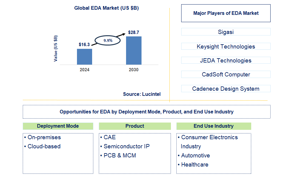
Key data points: The market size in 2030 = $28.7 billion, growth forecast = 9.9% annually for the next 6 years. Scroll below to get more insights. This market report covers trends, opportunities, and forecasts in the global eda market to 2030 by deployment mode (on-premises and cloud-based), product (CAE, semiconductor IP, and PCM & MCM), end use industry (consumer electronics industry, automotive, and healthcare), and region (North America, Europe, Asia Pacific, and the Rest of the World)
We'll send your sample report shortly.
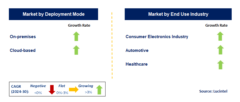
• Lucintel forecasts that, within the deployment type category, on-premises is expected to witness higher growth over the forecast period due to handling intricate chip designs, vast datasets, and uniformly transition to new operational processes for chip design, manufacturing, and verification with minimal risk and complexity in its management.
• Within this end-use category, consumer electronics will remain the largest segment due to the high adoption of advanced gadgets such as smart TVs and smartphones.
• In terms of regions, APAC is expected to witness the highest growth over the forecast period due to the strong position of the semiconductor industry in countries such as China, Japan, South Korea, and Taiwan. A more than 150-page report is developed to help in your business decisions.
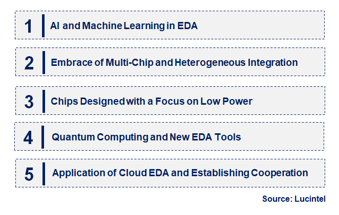
• AI and Machine Learning in EDA: AI is not just a buzzword; it is a game-changer, especially for EDA tools. AI can speed up the design process and mitigate potential problems during the design stage autonomously. This technology enables faster and easier chip layout optimization, involving many variables. AI in EDA tools allows design engineers to access data more quickly during the development process, which ultimately benefits the designs of modern semiconductors.
• Embrace of Multi-Chip and Heterogeneous Integration: The growing complexity of designs has led to a trend toward multi-chip and heterogeneous integration. EDA tools are evolving to support the design of systems that feature multiple chips working together. These tools help optimize the interaction between components, addressing performance, power, and size requirements. This trend is becoming increasingly important in technologies such as AI, IoT, and 5G, where multi-chip systems are gaining traction.
• Chips Designed with a Focus on Low Power Consumption: The increasing use of mobile devices and the growth of edge computing are driving the demand for power-efficient chips, which have become a priority in the EDA market. New EDA tools incorporate features like power analysis and optimization, allowing designers to create chips with high performance and low power consumption. These developments are crucial for industries like consumer electronics and automotive, where energy efficiency is a priority.
• Quantum Computing and New EDA Tools: The field of quantum computing is driving the development of new EDA tools tailored to quantum chip design. These tools address the challenges of developing quantum circuits that control and optimize qubits. As quantum computing becomes more feasible, the demand for EDA systems suited for quantum applications is expected to grow significantly.
• Application of Cloud EDA and Establishing Cooperation: There is a growing trend toward adopting cloud-based EDA tools, which create scalable, collaborative environments for chip design teams. Cloud-based platforms offer remote access, eliminate the need for expensive local infrastructure, and improve collaboration among different teams. These tools are particularly beneficial for smaller startups and design firms, as they provide access to software without incurring high capital costs. The EDA market is being revolutionized by emerging trends such as the integration of AI, multi-chip design, power-efficient chips, quantum computing, and cloud-based design collaboration. These developments are enabling faster and more efficient chip design processes that align with the growing needs of advanced semiconductor manufacturing. As these trends unfold, they will lead to the next generation of EDA tools, helping to meet the challenges associated with advanced chip design and manufacturing.
• AI-enabled Design Automation: Artificial intelligence is transforming the design automation process with AI-powered tools. These tools use machine learning algorithms to perform tedious tasks, optimize chip placement, and anticipate design issues. This integration accelerates the design cycle and enhances the quality of designs, particularly in complex semiconductor products such as 5G chips and AI processors.
• Emergence of Cloud-based EDA Platforms: With the growing demand for cloud-based EDA platforms, semiconductor design teams now have the option of working in flexible, scalable, and cost-efficient environments. Cloud solutions reduce capital expenses by eliminating the need for expensive local infrastructure, and they enhance collaboration among global teams, making the design process more flexible and efficient.
• Creation of Specialized EDA Tools for 5G Chip Design: Alongside the evolution of 5G technologies, there is an increasing demand for EDA tools that enhance the design of 5G chips. These tools focus on meeting the functional requirements of 5G chips, including high-speed data processing and low power consumption. EDA providers are upgrading their tools to accommodate the unique demands of 5G technology, helping manufacturers reduce lead times for 5G-capable products.
• Development of Tools Focused on Energy-efficient Design: With growing concerns about global warming and the proliferation of IoT devices, there is a global push toward energy-efficient designs. New EDA tools are being developed to support better power management, allowing designers to optimize power consumption during the entire design phase. This is particularly important for mobile devices, electric vehicles, and industries focused on energy efficiency.
• Management of Multi-chip Solutions and Advanced Packaging Designs: EDA tools have evolved to support advanced packaging designs, such as System-in-Package (SiP) and 3D packaging, which house multiple chips within a single unit. These advancements are crucial for designing high-performance chips and systems in smaller packages. As the demand for advanced multi-chip designs grows, EDA tools are adapting to the new requirements of 3D packaging. These changes are accelerating chip design processes and addressing the complexities of modern semiconductor products. As these developments continue, they will shape the future of semiconductor design and manufacturing, supporting new technologies like 5G and AI.
• AI and Machine Learning Chip Design: There is growing demand for machine learning algorithms, which is creating a need for specialized chips. This is driving interest in EDA tools that assist AI architects working with custom-built chip architectures. This segment presents significant growth opportunities for EDA providers targeting AI and machine learning applications.
• 5G and Telecom Infrastructure: The demand for building 5G networks is creating a need for differentiated EDA tools. These tools optimize the design of 5G chips, which require high-speed data processing and low latency. As investments in telecom infrastructure expand, EDA providers focusing on 5G chip design will see vast growth potential.
• Automotive and Autonomous Vehicles: Semiconductor chips are essential for electric vehicles, autonomous driving systems, and advanced driver-assistance systems. The automotive industry is increasingly relying on EDA tools for designing electronic chips, sensors, cameras, and radar systems. This trend presents an opportunity for EDA providers to serve the growing automotive semiconductor market.
• Quantum Computing: Moving towards New Frontiers: Chip design in quantum computing is an emerging research area, requiring specialized EDA tools. As research in quantum computing advances, there is a growing need for tools to optimize quantum circuits and control quantum bits (qubits). This new field offers a significant market opportunity for EDA providers developing tools for quantum processor design.
• Consumer Electronics and IoT Devices: With the rise of IoT and the increasing demand for consumer electronics like smartphones, wearables, and smart home devices, there is a high demand for advanced semiconductor designs. The market for IoT applications and consumer electronics offers significant growth potential, thanks to the availability of EDA tools that assist in designing large, low-power integrated circuit (IC) chips. Growth opportunities in AI chip design, 5G network architecture, automotive applications, quantum computing, and IoT are key drivers of the EDA market. By leveraging these opportunities, EDA providers can expand their market presence and meet the demands of advanced semiconductor designs. As industries evolve, the role of EDA tools in shaping future electronics and technologies will be crucial.
• Increasing Complexity of Semiconductor Designs: As devices become more advanced, the complexity of semiconductor designs increases. This requires more sophisticated EDA tools capable of handling multi-chip designs, 3D packaging, and AI optimization.
• Growth of AI and Machine Learning Applications: The rise of AI and machine learning is one of the primary drivers of the EDA market. The need to process vast datasets and develop specialized AI chips is pushing EDA tools to evolve.
• Expansion of 5G Networks: The deployment of 5G networks is driving new requirements for chip designs capable of handling augmented processing capabilities with low latency. The demand for EDA tools that optimize 5G chip configurations is increasing.
• The Demand for Power-efficient Designs: The growing popularity of smaller devices like phones and IoT devices, as well as electric vehicles, is increasing the demand for energy-efficient chips. EDA tools are adapting to meet these challenges by integrating power optimization techniques.
• Movement towards Cloud-Based EDA Tools: The rise of cloud computing has led to the growth of cloud-based EDA tools, which are flexible, scalable, and cost-efficient. These tools promote collaboration and make chip design more accessible to smaller firms and startups. Challenges in the EDA market are:
• High R&D Costs and Long Development Cycles: The development of new EDA tools requires significant investment in R&D. High costs and lengthy development times can pose challenges to smaller players in the market.
• Intellectual Property (IP) Protection: As EDA tools are proprietary software, intellectual property concerns can limit collaboration and slow down innovation.
• Complex Regulations and Standards: The semiconductor industry is subject to various regulations, including export controls and intellectual property laws. Navigating these regulations can be challenging for EDA providers. Despite these challenges, the market remains positive, with growth driven by innovation in chip design and manufacturing.
• Sigasi
• Keysight Technologies
• JEDA Technologies
• CadSoft Computer
• Cadenece Design System
• Silvaco International
• Mentor Graphics
• On-premises
• Cloud-based
• CAE
• Semiconductor IP
• PCB & MCM
• Consumer Electronics Industry
• Automotive
• Healthcare
• North America
• Europe
• Asia Pacific
• The Rest of the World
• United States: The majority of companies using computer-aided design (EDA) tools are based in the US. Synopsys, Cadence, and Mentor Graphics are some of the most important brands in the industry. In recent years, there has been a trend toward integrating AI and machine learning tools into EDA software. This enables chip engineers to design and manufacture chips more quickly and accurately. Additionally, there are now improved tools for designing chips for 5G and AI, driven by the need for faster semiconductors required by industries such as telecommunications, automotive, and cloud computing.
• China: One of the key advancements in the Chinese EDA sector is its self-reliant semiconductor policies. The government is funding the development of EDA software to reduce dependency on foreign tools. More local companies are now developing conceptual EDA solutions for semiconductor design, with a focus on national industries in sectors such as 5G, AI, and automotive. Additionally, China is promoting the development of chip design tools through several projects aimed at strengthening the country’s technology ecosystem.
• Germany: Germany has been advancing in the EDA market with a focus on automotive and industrial applications. With growing demand, German companies are now concentrating on e-chip designs for the electric vehicle market and self-driving technology. Moreover, Germany is increasing its research in quantum computing due to the rapidly growing need for specialized EDA tools for designing quantum chips. Such policies toward future technologies are helping Germany strengthen its competitive position in the global EDA market.
• India: The Indian semiconductor industry is starting to take off, and with this progress, EDA tools are becoming increasingly popular. The country is transforming into a design and testing service provider. With government policies supporting semiconductor manufacturing and design, EDA tools have gained significant traction, positioning India at the heart of the global EDA ecosystem. Domestic advancements are also stimulating further progress in this area.
• Japan: Japan is focusing on next-generation chip devices, with EDA tools reaching multinational companies. Industries like robotics, automotive, and consumer electronics require cutting-edge chips, and Asia is targeting these sectors as promising markets. Japan has developed EDA software specifically for precision industries to improve microelectronics design. Furthermore, Japanese companies are integrating AI and machine learning into EDA tools to reduce design cycles for complex systems, thus improving process capabilities through software integration.

• Sigasi
• Keysight Technologies
• JEDA Technologies
• CadSoft Computer
• Cadenece Design System
• Silvaco International
• Mentor Graphics Q6. Which EDA market segment will be the largest in future? Answer: Lucintel forecasts that on-premises is expected to witness higher growth over the forecast period due to handling intricate chip designs, vast datasets, and uniformly transition to new operational processes for chip design, manufacturing, and verification with minimal risk and complexity in its management. Q7. In EDA market, which region is expected to be the largest in next 5 years? Answer: APAC is expected to witness the highest growth over the forecast period due to the strong position of the semiconductor industry in countries such as China, Japan, South Korea, and Taiwan. Q.8 Do we receive customization in this report? Answer: Yes, Lucintel provides 10% customization without any additional cost.


Choose a license that fits your team. Instant PDF delivery.
Prices exclude taxes. Instant delivery. Custom licensing available on request.
Market Report · July 24, 2026
Market Report · July 20, 2026
Market Report · July 20, 2026
Trusted partner for strategic intelligence and business growth


Receive a complimentary market analysis tailored to your industry. Our analysts will identify key growth opportunities and competitive dynamics specific to your business.

Market size, growth rate, and key trend analysis for your specific sector.

Top competitor positioning and market share analysis.

Strategic recommendations backed by data-driven insights.
Get curated market intelligence and competitive moves straight to your inbox.
By subscribing, you agree to receive our monthly insights. Unsubscribe anytime.
Receive a complimentary market analysis tailored to your industry. Our analysts will identify key growth opportunities and competitive dynamics specific to your business.
Market size, growth rate, and key trend analysis for your specific sector.
Top competitor positioning and market share analysis.
Strategic recommendations backed by data-driven insights.
Get curated market intelligence, emerging trends, and competitive moves straight to your inbox each month.
By subscribing, you agree to receive our monthly insights. Unsubscribe anytime.
We'll send your sample report shortly.