
Market Report · May 18, 2026

This market report covers trends, opportunities, and forecasts in the global dry etching system market to 2031 by technology (reactive ion etching (rie) systems and deep reactive ion etching (drie) systems), application (semiconductor industry, medical industry, electronics & microelectronics, and others), and region (North America, Europe, Asia Pacific, and the Rest of the World)
We'll send your sample report shortly.
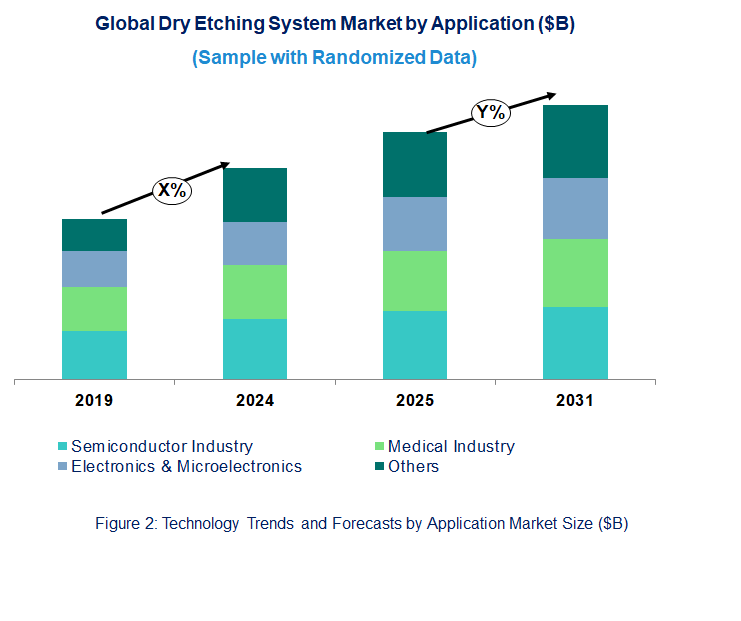
• Shift Toward Atomic Layer Etching (ALE): Atomic Layer Etching (ALE) is gaining momentum due to its ability to offer angstrom-level precision and minimize substrate damage. As nodes shrink below 5nm, ALE becomes critical for ensuring high selectivity and uniformity, supporting next-gen chip designs and improving yield rates.
• Integration with EUV Lithography: Dry etching systems are increasingly being developed to complement Extreme Ultraviolet (EUV) lithography processes. As EUV becomes essential for advanced nodes, compatible etching technologies must ensure accurate pattern transfer and manage new challenges such as line edge roughness and pattern fidelity.
• Use of AI and Machine Learning in Process Control: Manufacturers are integrating AI and machine learning algorithms to optimize etching parameters in real time. These tools enhance process repeatability, reduce cycle times, and increase throughput, especially in high-volume fabs handling diverse chip architectures.
• Growing Demand for Compound Semiconductor Etching: The rise in applications using GaN, SiC, and other compound semiconductors—such as EVs, 5G, and power electronics—is driving the need for dry etching systems tailored to these materials. Customized etching processes that address unique material properties are increasingly in demand.
• Environmental and Energy Efficiency Innovations: With growing emphasis on sustainability, dry etching system manufacturers are innovating to reduce greenhouse gas emissions, energy use, and chemical consumption. Developments include low-temperature etching techniques and improved vacuum and gas management systems. These emerging trends reflect the ongoing evolution of the dry etching system market in response to semiconductor industry demands for greater precision, material diversity, and sustainable operations. As manufacturers strive to produce faster, smaller, and more efficient chips, these advancements are crucial in redefining the capabilities of etching technologies and reshaping the global semiconductor landscape.
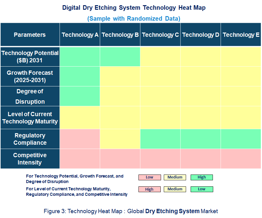
• Technology Potential: The dry etching system market holds substantial technological potential, particularly in enabling next-generation semiconductor manufacturing. Its ability to deliver high precision, anisotropic etching, and compatibility with advanced materials like GaN and SiC make it indispensable for fabricating chips at sub-5nm nodes. Technologies like Atomic Layer Etching (ALE) and plasma-enhanced etching enhance etching accuracy down to the atomic level, supporting complex 3D architectures such as FinFETs and gate-all-around (GAA) transistors.
• Degree of Disruption: The degree of disruption is high, as dry etching systems are critical enablers of Extreme Ultraviolet (EUV) lithography and the move toward smaller, more powerful, and energy-efficient devices. As semiconductor nodes shrink and demand for heterogeneous integration rises, dry etching continues to replace many traditional wet etching processes.
• Current Technology Maturity Level: In terms of technology maturity, mainstream dry etching techniques (like reactive ion etching) are well-established, but next-gen variants (such as ALE and cryogenic etching) are still evolving. These newer methods are in early-to-mid adoption stages among leading-edge fabs.
• Regulatory Compliance: Regulatory compliance is increasingly important due to the use of hazardous gases and energy-intensive processes. Manufacturers must comply with environmental safety standards, such as RoHS and REACH, and adopt energy-efficient and low-emission systems to align with global sustainability goals and fab cleanroom protocols.
• Hitachi High-Tech: Launch of DCR Etch System 9060 Series: Hitachi High-Tech introduced the DCR Etch System 9060 Series, designed for precise isotropic etching at the atomic level. This system addresses the challenges of fabricating high-aspect-ratio 3D structures in advanced semiconductor devices, such as 3D-NAND and 3D-DRAM. By enabling rapid temperature modulation within a single vacuum reactor, the 9060 Series enhances throughput and reduces equipment footprint, supporting both R&D and mass production environments.
• Plasma-Therm: Advancements in Plasma Dicing and Material Processing: Plasma-Therm has been at the forefront of plasma processing technology, offering innovative solutions like plasma dicing-on-tape, which revolutionizes die separation for thin and ultra-thin wafers. Their Singulator® platform minimizes physical damage during dicing, crucial for power devices and photonics applications. Additionally, Plasma-Therm's focus on material modernization and integration of AI for process optimization underscores their commitment to addressing complex manufacturing needs across various semiconductor segments.
• Samco: Expansion into European Market with Advanced ICP-RIE Systems: Samco announced the sale of its advanced ICP-RIE systems, RIE-400iP, to III-V Lab in France. These systems are tailored for processing III-V compound semiconductors like InP, GaN, and GaAs, supporting research and development in optoelectronic and microelectronic components. The collaboration signifies Samco's strategic expansion into the European market and its commitment to advancing compound semiconductor technologies.
• Plasma Etch: Enhancing Etching Capabilities for Diverse Applications: Plasma Etch continues to innovate in the dry etching domain, focusing on customizable solutions for various applications, including MEMS, photonics, and advanced packaging. Their systems are designed to provide precise etching with high uniformity, catering to the nuanced requirements of modern semiconductor fabrication processes. By emphasizing flexibility and precision, Plasma Etch supports the industry's move towards more complex and miniaturized devices. These developments reflect the dynamic nature of the dry etching system market, where continuous innovation is essential to meet the demands of next-generation semiconductor manufacturing. As companies like Hitachi High-Tech, Plasma-Therm, Samco, and Plasma Etch advance their technologies, they play a pivotal role in shaping the future of electronics by enabling more efficient, precise, and adaptable fabrication processes.
• Demand for Advanced Semiconductor Devices: The increasing production of high-performance, smaller, and more efficient semiconductor devices fuels the need for precise dry etching systems. This growth drives innovation in etching technology to achieve finer patterns and higher aspect ratios.
• Growth in MEMS and Microelectronics: Expansion of MEMS applications in automotive, medical, and consumer electronics sectors increases demand for specialized dry etching solutions that enable complex 3D structures with high precision.
• Rising Adoption of DRIE Technology: DRIE systems are gaining traction due to their ability to create deep, anisotropic etch profiles critical for advanced packaging and sensor technologies, boosting market growth through enhanced process capabilities. Key Challenges:
• Stringent Environmental and Safety Regulations: Compliance with evolving regulations on chemical use and emissions necessitates the development of eco-friendly and safe dry etching processes, encouraging innovation but also increasing operational costs.
• High Capital and Operational Costs: The complexity and expense of dry etching equipment limit adoption among smaller manufacturers and slow market expansion in price-sensitive regions.
• Technical Complexity and Process Integration: Integrating dry etching systems with existing semiconductor manufacturing lines requires specialized expertise, posing challenges in deployment and scalability.
• Supply Chain and Raw Material Constraints: Dependence on specialized gases and materials exposes the market to supply disruptions, impacting production schedules and costs. In summary, while drivers like semiconductor innovation and MEMS growth propel the dry etching system market forward, challenges including high costs, regulatory pressures, and integration complexity must be managed. These dynamics are shaping the market’s evolution and driving continuous technological advancement.
• Hitachi High-Technologies
• Plasma-Therm
• Spts Technologies
• Samco
• Plasma Etch
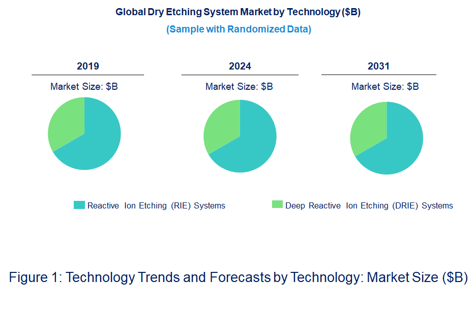
• Technology Readiness by Technology Type: Reactive ion etching (RIE) is a mature and widely adopted technology with high readiness across global semiconductor fabs, supporting logic, memory, and display manufacturing. Deep reactive ion etching (DRIE), while less mature, is quickly advancing due to demand in MEMS, TSVs, and 3D integration applications. RIE benefits from established supply chains and regulatory frameworks, while DRIE requires more stringent compliance due to deeper etching and more complex gas processes. Both technologies are becoming increasingly competitive through innovations in process automation and plasma control. RIE is versatile and integrated across multiple node sizes, while DRIE is gaining momentum in high-growth applications like automotive sensors and biomedical devices. Government-supported research and development is helping accelerate DRIE’s technology maturity. As device architectures become more complex, both technologies are evolving rapidly. Their growing integration into advanced manufacturing highlights strong readiness and future potential.
• Disruption Potential: The dry etching system market is being transformed by the disruptive impact of reactive ion etching (RIE) and deep reactive ion etching (DRIE) technologies. RIE offers precise anisotropic etching, replacing wet etching in semiconductor fabrication, while DRIE enables high-aspect-ratio structures critical for MEMS and 3D ICs. As device miniaturization and complexity grow, both technologies become essential for advanced manufacturing. RIE remains widely used in mainstream processes, while DRIE is emerging as a key enabler in advanced packaging, IoT, and automotive sensors. Integration with atomic layer etching enhances both systems’ capabilities. The push toward smaller nodes and better performance boosts demand for these technologies. Innovations in plasma control and selectivity further drive disruption. With new applications and higher etching precision, RIE and DRIE systems are reshaping next-generation semiconductor production.
• Competitive Intensity and Regulatory Compliance: RIE and DRIE systems face intense competition in the dry etching system market, with numerous players striving for innovation, efficiency, and cost advantages. RIE is broadly adopted and highly competitive, while DRIE is gaining ground due to its relevance in niche but expanding sectors. Companies are differentiating through proprietary etch processes, chamber designs, and service offerings. At the same time, regulatory compliance is critical due to the use of hazardous gases and vacuum processes. DRIE faces more regulatory scrutiny because of its complex etching requirements. Environmental standards, including SEMI and ISO, shape market access and technology development. Vendors are investing in cleaner technologies and gas recycling systems to meet sustainability demands. Trade regulations, particularly between the U.S. and Asia, also influence competition. Regulatory compliance is now a strategic factor in maintaining market leadership alongside technological innovation.
• Reactive Ion Etching (RIE) Systems
• Deep Reactive Ion Etching (DRIE) Systems
• Semiconductor Industry
• Medical Industry
• Electronics & Microelectronics
• Others
• North America
• Europe
• Asia Pacific
• The Rest of the World
• Latest Developments and Innovations in the Dry Etching System Technologies
• Companies / Ecosystems
• Strategic Opportunities by Technology Type


Choose a license that fits your team. Instant PDF delivery.
Prices exclude taxes. Instant delivery. Custom licensing available on request.
Market Report · May 18, 2026
Market Report · May 18, 2026
Market Report · May 18, 2026
Trusted partner for strategic intelligence and business growth


Receive a complimentary market analysis tailored to your industry. Our analysts will identify key growth opportunities and competitive dynamics specific to your business.

Market size, growth rate, and key trend analysis for your specific sector.

Top competitor positioning and market share analysis.

Strategic recommendations backed by data-driven insights.
Get curated market intelligence and competitive moves straight to your inbox.
By subscribing, you agree to receive our monthly insights. Unsubscribe anytime.
Receive a complimentary market analysis tailored to your industry. Our analysts will identify key growth opportunities and competitive dynamics specific to your business.
Market size, growth rate, and key trend analysis for your specific sector.
Top competitor positioning and market share analysis.
Strategic recommendations backed by data-driven insights.
Get curated market intelligence, emerging trends, and competitive moves straight to your inbox each month.
By subscribing, you agree to receive our monthly insights. Unsubscribe anytime.
We'll send your sample report shortly.