
Market Report · July 24, 2026

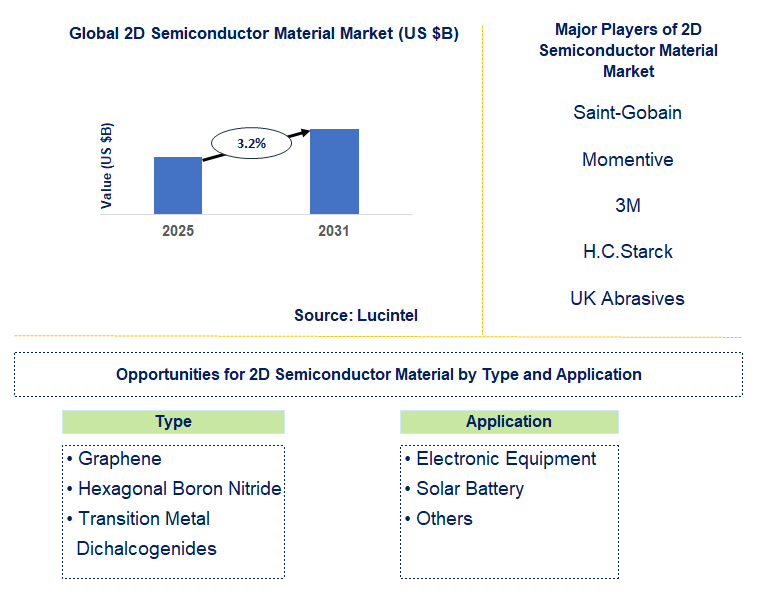
Key data points: The growth forecast = 3.2% annually for the next 7 years. Scroll below to get more insights. This market report covers Trends, opportunity and forecast in 2D semiconductor material market to 2031 by type (graphene, hexagonal boron nitride, and transition metal dichalcogenides), application (electronic equipment, solar battery, and others), and region (North America, Europe, Asia Pacific, and the Rest of the World)
We'll send your sample report shortly.
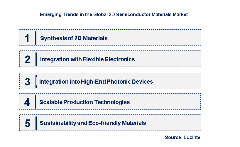
• Synthesis of 2D Materials: Researchers are finding new ways to synthesize high-quality 2D materials, including graphene, TMDs, and black phosphorus. The techniques used are chemical vapor deposition (CVD) and liquid-phase exfoliation methods, which will allow for the development of higher material performance, scalability, and cost-effectiveness. Synthesis is crucial to meeting the ever-growing demand for 2D semiconductors in electronics, energy storage, and photonics.
• Integration with Flexible Electronics: The interest in integrating 2D semiconductor materials with flexible electronics is on the rise. Demand for light-weight, stretchable, and bendable electronic devices at each application level from wearables to smart textiles and sensors can explain this trend. 2D semiconductor materials, which have excellent mechanical properties with good electrical conductivity, drive this interest. There is expected to be growth due to the combination of flexibility and functionality.
• Integration into High-End Photonic Devices: TMDs and other 2D materials are gradually being exploited for photonic devices, including LEDs, photodetectors, and lasers. TMD-based products possess outstanding optoelectronic characteristics, leading to the development of extremely fast and efficient devices. The prospect of employing 2D materials in high-speed communication and quantum computing extends the trend further. Research on using them in photonics is gaining momentum, opening up promising growth opportunities.
• Scalable Production Technologies: Scalable production technologies are used to provide an answer to the increasing worldwide demand for 2D materials. Roll-to-roll printing, among other large-area growth techniques, is now considered to develop large-scale and inexpensive production for graphene and many other 2D materials. Scalable production is a prime need for making widespread commercial use of 2D semiconductors, especially in consumer electronics and industries.
• Sustainability and Eco-friendly Materials: The demand for environmentally sustainable and energy-efficient materials is driving innovation in the 2D materials market. Researchers are investigating ways to make production processes more eco-friendly and to develop 2D materials that can be integrated into energy-efficient devices. This trend reflects growing global interest in sustainable technologies and the potential for 2D materials to contribute to greener electronics and energy solutions. These growing trends are thus changing the nature of the 2D semiconductor material market in terms of innovating and exploring new avenues of growth. Research in material synthesis, flexible integration of electronics, photonic, scalable production and sustainability are aspects that are gaining momentum in bringing growth to this market. While these trends emerge, they tend to bring into the industry quite a few monumental technological breakthroughs and economic growth opportunities.
• High-quality graphene: The development of high-quality graphene materials for next-gen electronics has been one of the most significant achievements in this field. This includes advancements in synthesis techniques, such as chemical vapor deposition (CVD) and liquid-phase exfoliation, which allow for the production of large-area graphene sheets. The improved quality of graphene has opened up new applications in flexible electronics, energy storage, and high-speed communication.
• Growth of TMDs for Semiconductor Applications: Transition metal dichalcogenides (TMDs) have gained attention for their potential in semiconducting applications. Advances in TMD material properties, including high electron mobility and tunable bandgaps, have made them ideal candidates for use in field-effect transistors, optoelectronic devices, and flexible sensors. Research is focusing on improving the scalability and cost-effectiveness of TMD production to bring them into commercial use.
• Quantum Computing: 2D semiconductor materials are being considered for quantum computing applications, where their unique properties may play a critical role in improving the performance of quantum bits (qubits). Researchers are studying how materials like graphene and TMDs can be integrated into quantum devices to enable faster, more stable quantum computations. This is one of the promising frontiers for 2D materials in the technology sector.
• Large Scale Production Techniques: In order to cater to worldwide demand, research and development focus on cost-effective scalable production techniques for 2D semiconductors is growing. Recent breakthroughs in roll-to-roll printing, chemical vapor deposition, and laser-assisted methods facilitate large-scale 2D material production. It will be of paramount importance for lowering the costs and making these materials more available in consumer electronics, automotive, and industrial fields.
• Improved Material Properties for Flexible Electronics: Scientists are working to enhance the properties of 2D materials for flexible electronics. They are focusing on improving the mechanical properties, conductivity, and flexibility of 2D materials. Advances in material doping, composite structures, and surface treatments are enabling the development of more reliable and durable flexible electronic devices. These improvements will open up new markets for 2D materials in wearables, health monitoring, and IoT devices. The new advances in 2D semiconductor materials are helping foster growth and innovation. Improved quality of material, techniques for its production, and various applications have paved the way for more commercialization. This will be going to unlock newer opportunities across many industries as developments progress ahead; they will facilitate faster in the adoption of 2D semiconductor materials in advanced technologies.
• Flexible Electronics: The need for flexible and wearable electronics is growing at a rapid pace. 2D materials such as graphene and transition metal dichalcogenides will exhibit flexibility, superior electrical conductivity, and lightweight design, making them highly suitable for wearable applications, healthcare tracking, and intelligent textiles. Scalable production of these 2D materials would accelerate mass adoption, developing huge market opportunities.
• Energy Storage Solutions: The 2D material, graphene can be one of the possible ways to enhance the energy storage devices such as supercapacitors and batteries. On account of a high surface area of high electrical conductivity, they are thereby found as ideal candidates for enhancing energy storage systems. In the future, the demand for energy storage in electric vehicles along with renewable energy is ever increasing.
• Optoelectronics and Photonics: Interest in using 2D materials in optoelectronics, such as LEDs, photodetectors, and lasers, is great. These materials have excellent optical properties that make for faster, more efficient devices for communication, sensing, and display technologies. Demand for high-performance photonic devices is growing rapidly and driving the use of 2D materials in advancing next-generation photonics.
• Quantum Computing: There is an increased interest in the use of 2D materials for quantum computing applications. The properties of 2D materials, such as high electron mobility and tunable electronic behavior, make them very suitable for the implementation of quantum devices, such as qubits. With the expansion of the quantum computing industry, 2D materials represent a critical enabling technology to enhance the speed and efficiency of quantum processors.
• Sensors and IoT Applications: The rapid growth of the Internet of Things (IoT) and sensor technology is providing new avenues for 2D materials. The high sensitivity and flexibility of these materials make them suitable for applications in sensors to detect environmental changes, biological signals, or chemical interactions. Demand for IoT devices is increasing exponentially, and thus, 2D materials are going to be critical in the development of sophisticated sensors for smart cities, industrial automation, and healthcare applications. Strategic growth opportunities in 2D semiconductor materials are scattered over various applications in flexible electronics, energy storage, optoelectronics, quantum computing, and sensors. They are found through the extraordinary properties of 2D materials and are needed to be integral components of future next-generation technologies. As such, these applications would play an integral role in furthering the course of development in 2D semiconductors going forward.
• Saint-Gobain
• Momentive
• 3M
• H.C.Starck
• UK Abrasives
• Denka
• Henze
• Showa Denko Group
• Xinfukang
• Qingzhou Fangyuan
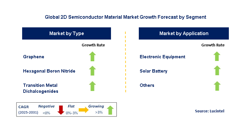
• Graphene
• Hexagonal Boron Nitride
• Transition Metal Dichalcogenides
• Electronic Equipment
• Solar Battery
• Others
• North America
• Europe
• Asia Pacific
• The Rest of the World
• United States: United States has developed significantly with the advancement of the 2D semiconductor material market, particularly on graphene and TMDs. The major research initiatives focused on enhancing the properties of these materials for application in next-generation transistors, photodetectors, and flexible electronics. The US-based companies are now also developing scalable production methods in order to address the growing demand. This way, the U.S. remains one of the innovation hotspots in the 2D semiconductor industry.
• China: China is also gaining pace in the 2D semiconductor material market as it invests a lot in research and development. The country has achieved advancements in developing high-quality graphene and other 2D materials for flexible display, sensor, and next-generation electronics. China is also focusing on large-scale production technologies, where it aims to dominate the supply chain of the entire world. The government’s support through funding and policy has really speeded up the growth of this market, putting China as a key competitor globally.
• Germany: Germany has significantly contributed to the development of 2D semiconductor materials, especially in material characterization and integration into industrial applications. German research institutions and corporations are at the forefront of exploring the potential of TMDs for high-performance semiconductors and photonics. Germany’s strong manufacturing base for electronics also plays a pivotal role in pushing forward the commercialization of 2D materials. This growing emphasis on material research positions Germany as a leader in the European market.
• India: The research of 2D semiconductor materials is still in the early stages for India, but there are efforts in both the academic and industrial sectors. Universities and institutions are working on cheaper production methods of 2D materials, specifically graphene. Potential growth areas in flexible electronics and energy storage can be expected to be very high. Further potential for the commercialization of 2D semiconductors lies in India’s expanding electronics manufacturing industry.
• Japan: Japan continues to lead in innovation in the 2D semiconductor material market. Companies based in Japan are actively driving innovations for the utilization of TMDs in high-speed transistors, flexible electronics, and advanced sensors, among other applications. The well-developed semiconductor industry in Japan complements growth in 2D materials through the encouragement of collaborations between research institutions and the private sector. Another critical investment area that Japan is pushing into is in advanced material synthesis and production technologies to maintain competitiveness.


• Saint-Gobain
• Momentive
• 3M
• H.C.Starck
• UK Abrasives
• Denka
• Henze
• Showa Denko Group
• Xinfukang
• Qingzhou Fangyuan Q5. Which 2D semiconductor material market segment will be the largest in future? Answer: Lucintel forecasts that graphene is expected to witness the highest growth over the forecast period due to its exceptional electrical conductivity. Q6. In 2D semiconductor material market, which region is expected to be the largest in next 5 years? Answer: APAC is expected to witness the highest growth over the forecast period due to high investments in electronics and renewable energy technologies. Q7. Do we receive customization in this report? Answer: Yes, Lucintel provides 10% customization without any additional cost.


Choose a license that fits your team. Instant PDF delivery.
Prices exclude taxes. Instant delivery. Custom licensing available on request.
Market Report · July 24, 2026
Market Report · July 20, 2026
Market Report · July 20, 2026
Trusted partner for strategic intelligence and business growth


Receive a complimentary market analysis tailored to your industry. Our analysts will identify key growth opportunities and competitive dynamics specific to your business.

Market size, growth rate, and key trend analysis for your specific sector.

Top competitor positioning and market share analysis.

Strategic recommendations backed by data-driven insights.
Get curated market intelligence and competitive moves straight to your inbox.
By subscribing, you agree to receive our monthly insights. Unsubscribe anytime.
Receive a complimentary market analysis tailored to your industry. Our analysts will identify key growth opportunities and competitive dynamics specific to your business.
Market size, growth rate, and key trend analysis for your specific sector.
Top competitor positioning and market share analysis.
Strategic recommendations backed by data-driven insights.
Get curated market intelligence, emerging trends, and competitive moves straight to your inbox each month.
By subscribing, you agree to receive our monthly insights. Unsubscribe anytime.
We'll send your sample report shortly.